Yesterday was the big day, AMD presented the RDNA3 architecture and the Radeon RX 7900 XT and Radeon RX 7900 XTX, two graphics cards that will be the most powerful models of the new generation of the Sunnyvale giant for the general consumer market. We already had enough information about them, in fact we made a compilation with the most reliable data of the Radeon RX 7000, and in the end most of the rumors that we had on the table have been fulfilled.
The Radeon RX 7900 XT and Radeon RX 7900 XTX use a chiplet-like architecture, but the GPU maintains a monolithic core design. It is important to make this distinction because RDNA3 does not use two interconnected GPUsbut integrates the GPU on a single chip, and this is interconnected with six chips that only house the L3 cachealso known as infinite cache.
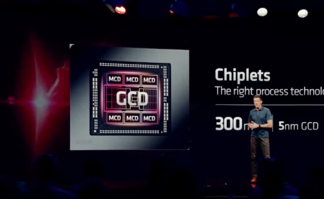
In the image we can clearly see that design, the GPU is located in the central package, which is the largest, and the L3 cache is spread across the six smaller packages that surround it. With this design, AMD has freed up significant space at the silicon level in the GPU, and without having to give up that infinite cache. Imagine the complexity it would have added to the GPU design, and the space it would have taken up, if all that cache had been integrated with the GPU on a single chip, and therefore in a single package.
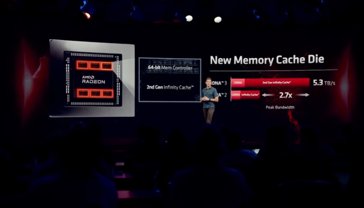
As we had already told you in previous information, the GPU block is known as GCD, or “Graphics Core Die”and the cache blocks are identified as “MCD”, or “multi-cache die”. The GPU is manufactured in the node of 5nmand each GCD uses the node of 6nm. The Navi 31 GPU has a total of 12,288 shaders, and each MCD adds 16 MB of infinite cache and also integrates a 64-bit memory controller. Since we have six GCD units we find 96 MB of L3 in total and with a 384-bit bus. The bandwidth of the infinite cache has a peak of 5.3TB/s.
The Radeon RX 7900 improve in power, efficiency and specialization
We have already seen that RDNA3 represents, just because of its design that externalizes the L3 cache, an important evolution compared to RDNA2, but the changes that this architecture brings go much further and deserve an in-depth analysis. AMD has been able to double the number of shaders per computing unit, which means we went from 64 shaders to 128 shaders. In this way, the Radeon RX 7900 XTX, which has 96 CUs, adds a total of 12,288 shaders. If the count of 64 shaders per CU had been maintained, it would only have 6,144 shaders.
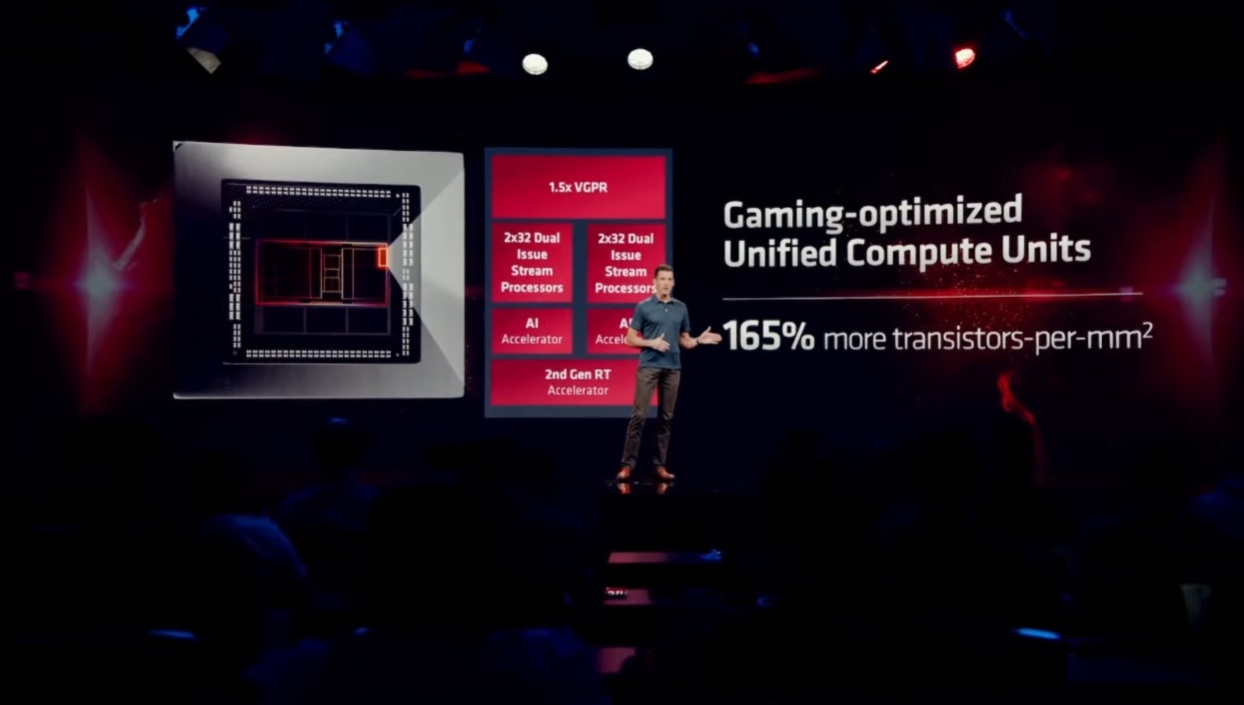
The jump from the 7nm to the 5nm node in the GPU is another of the most important novelties. Using a more advanced node allows for improved efficiency and transistor density, and also frees up space at the silicon level by reducing transistor size. That space that AMD has freed up at the silicon levelthanks to the 5nm node and the outsourcing of the L3 cache, has been optimally usedsince the Sunnyvale giant has confirmed that the Radeon RX 7900 XT and XTX integrate:
- Second generation ray tracing acceleration kernels.
- Artificial intelligence acceleration units.
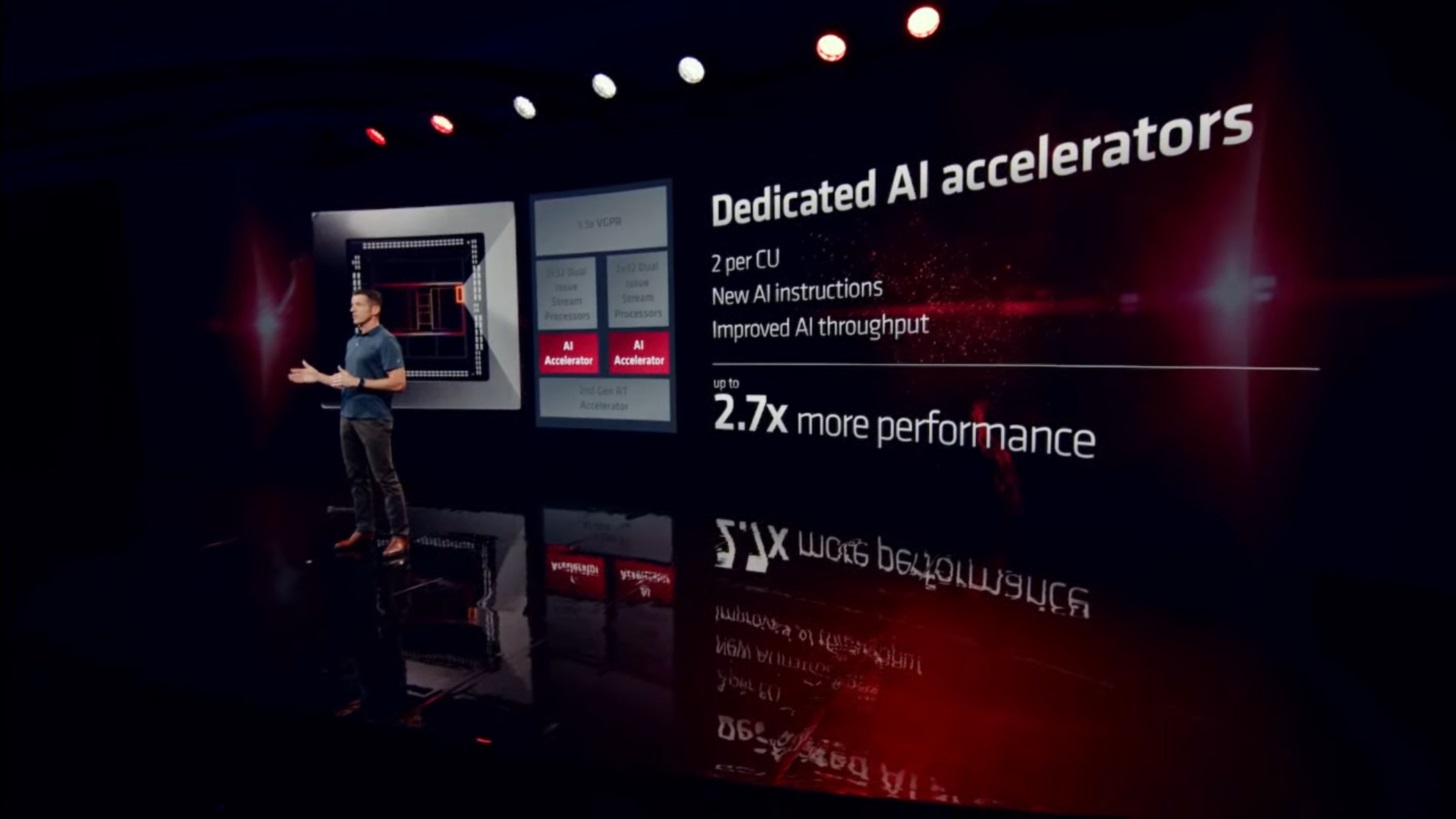
The Radeon RX 7900 XT and XTX are therefore the first graphics cards from AMD for general consumption that include specialized AI coresa component that we can think of as the equivalent of NVIDIA’s Tensor Cores and Intel’s XMX Arrays.
From what AMD showed during the presentation of both graphics cards, we can deduce that an RDNA3 compute unit consists of 128 shaders, two AI acceleration units, and a ray tracing accelerator. The number of texturing units per CU should be 4.
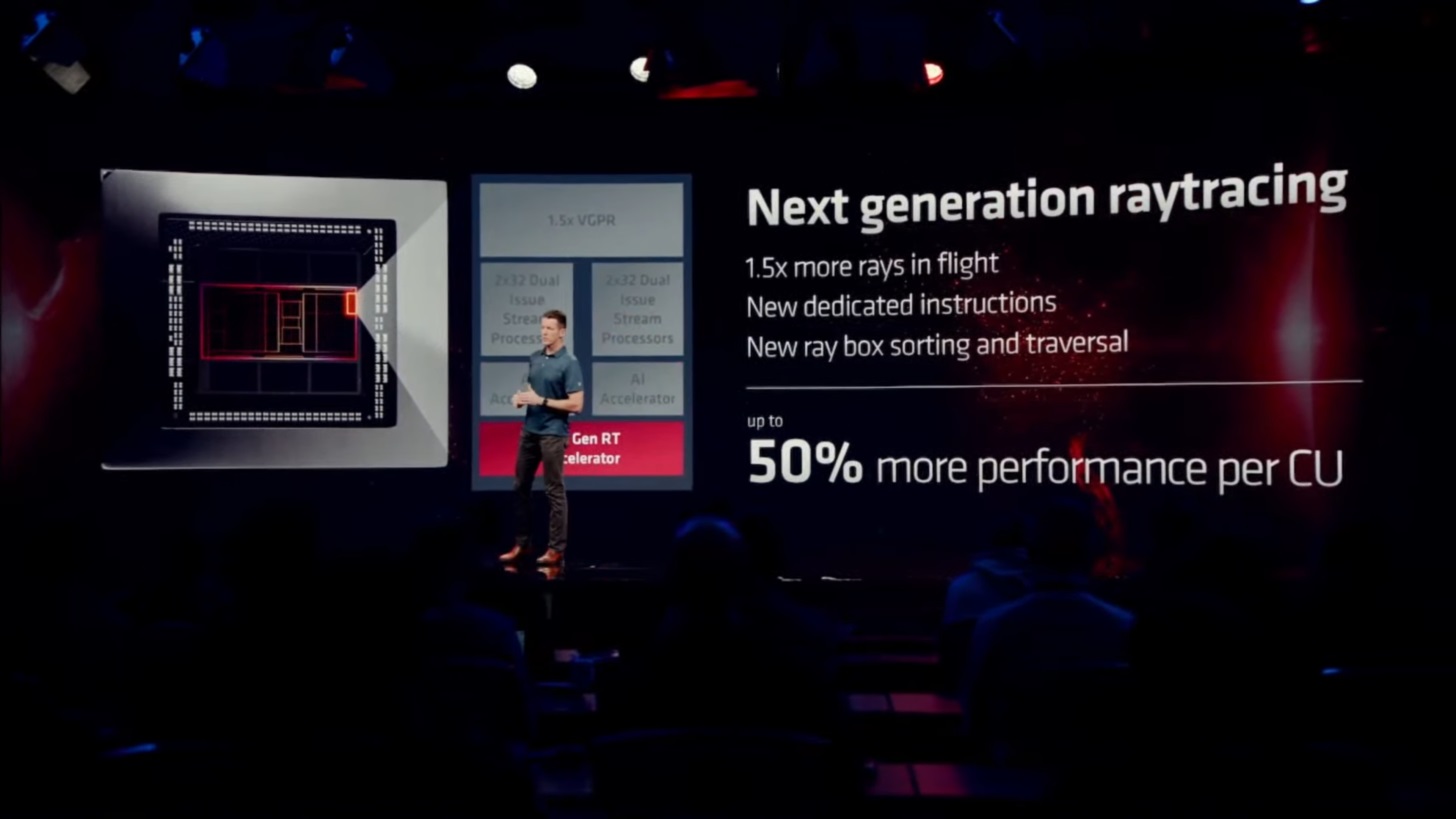
In theory, new ray tracing accelerators improve performance by 50% over the previous generationwhich means that the Radeon RX 7000 have taken an important generational leap in this regard compared to the Radeon RX 6000. The performance data that AMD has shared allows us to make a comparison with the GeForce RTX 4090 and the GeForce RTX 3090 Ti , and this are the results:
- In Cyberpunk 2077 With 4K resolution, maximum quality and ultra ray tracing the Radeon RX 7900 XTX achieves, with FSR activated in performance mode, 62fps. If AMD has used performance mode, that result lags behind the 67fps you get a GeForce RTX 3090 Ti with DLSS 2 in performance mode, and it’s a far cry from the 139fps that the GeForce RTX 4090 achieves with ray tracing in insane and DLSS 3 in performance mode.
- In Dying Light 2 With 4K resolution, maximum quality and ultra ray tracing the Radeon RX 7900 XTX achieves 72fps. Due to the enormous improvement that the FSR marks, we assume that it was configured in performance mode. With those same settings and DLSS 2 in performance mode a GeForce RTX 3090 Ti achieves 77fps on average, and a GeForce RTX 4090 reaches 130fps.
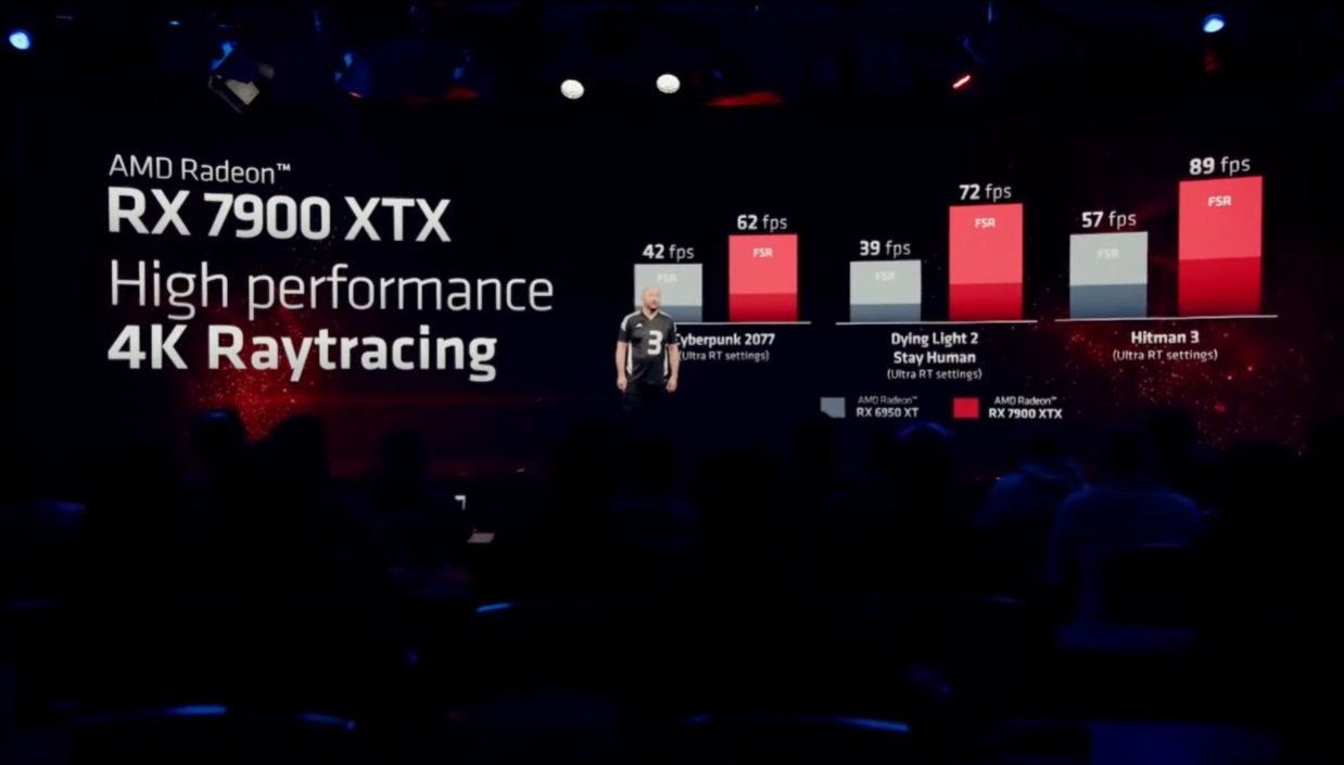
I wanted to make this comparison so that you have a more realistic idea of what we can expect from the Radeon RX 7900 XT and XTX in ray tracing, and yes, it is clear that Although we have an important generational improvement, the RDNA3 architecture is still not up to the level of the most advanced of NVIDIA if we talk about ray tracing. This was precisely one of the things that the Radeon RX 7000 needed to compete head-to-head with the GeForce RTX 40, improve ray tracing performance.
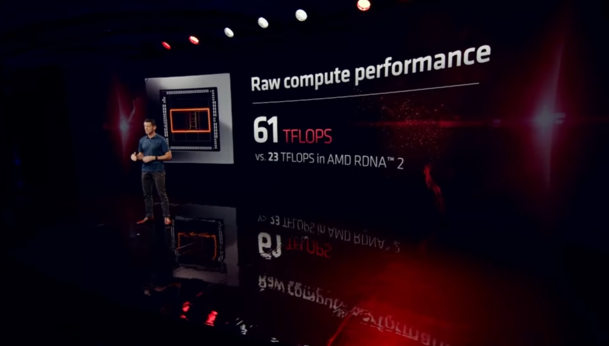
In terms of raw power AMD has confirmed that the Radeon RX 7900 XTX will peak at 61 TFLOPs. The RDNA3 architecture has improved efficiency by 54%and will be able to execute two instructions per clock cycle in the shaders. Another interesting detail is that AMD has differentiated the frequencies of the shaders and those of the front end, which will work at slightly different levels to “improve efficiency,” in the company’s own words.
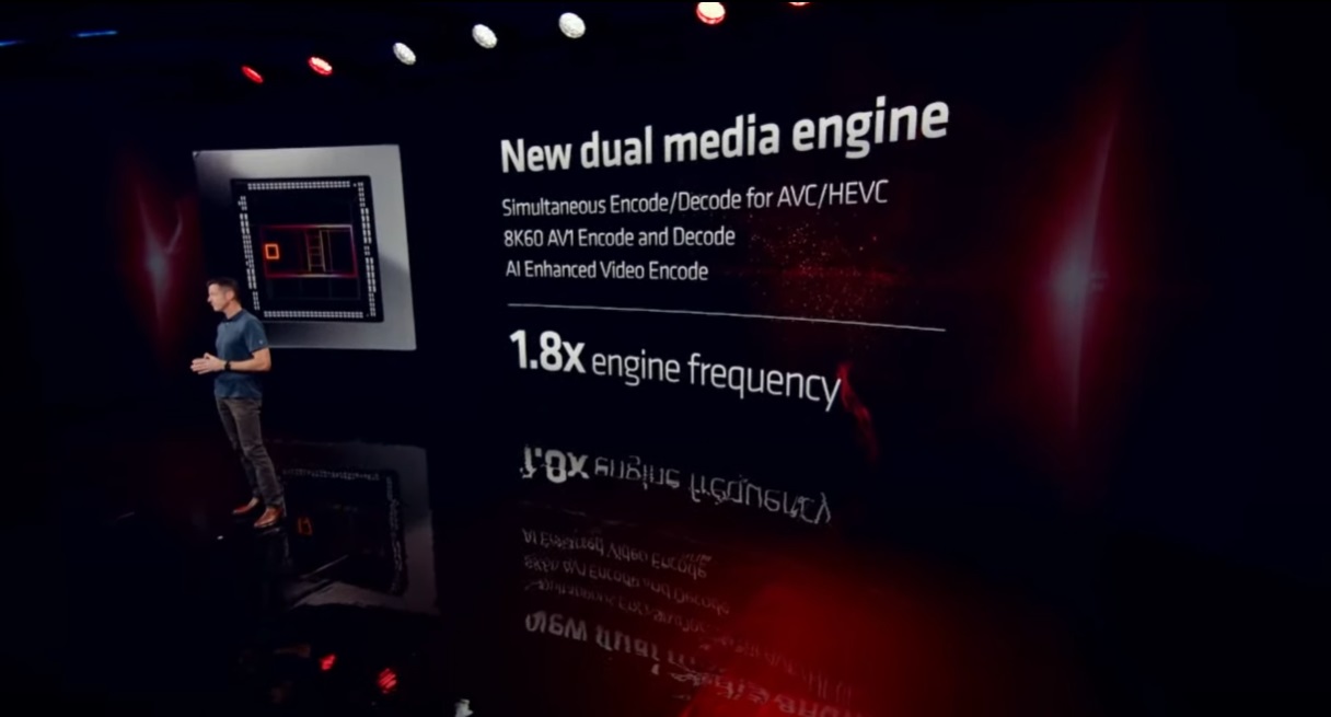
The Radeon RX 7900 XT and XTX support Simultaneous encoding and decoding under the AV1 standardand are also standards compliant DisplayPort 2.1 and HDMI 2.1awhich means that we can use them to play in 4K resolution with a refresh rate of up to 480 Hz, or in 8K with a refresh rate of up to 165 Hz.
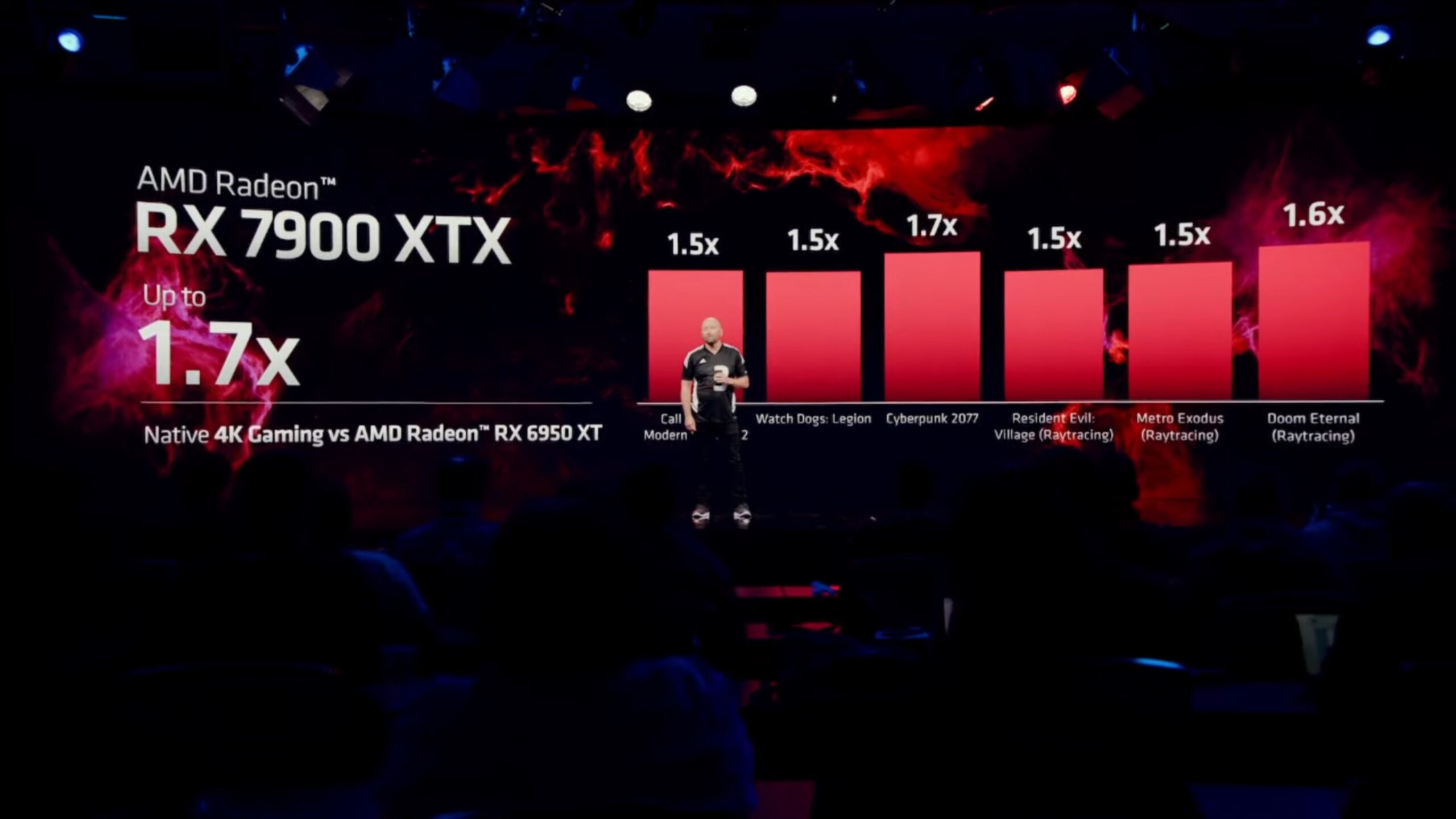
AMD also took the opportunity to compare the performance of the Radeon RX 7900 XTX against the Radeon RX 6950 XT, and it was clear what we can expect an improvement of between 50% and 70%, depending on the game used, with 4K resolution. In the attached graph we can see the titles used in the comparison.
Specifications, price and release date of the Radeon RX 7900 XT and XTX
Both graphics cards will be available from December 13th, and they will have a very similar price, which confirms that the performance differences between the two are going to be quite small. The Radeon RX 7900 XT will cost $899, and the Radeon RX 7900 XTX will be priced at $999. Keep in mind that in both cases they are prices without taxes, and that in Spain, after converting currency and applying taxes, would be equivalent to 1,110 euros and 1,213 euros.
Radeon RX 7900 XT Specifications
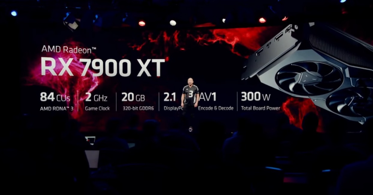
- Navi 31 graphics core with MCD (Multi-chiplet Die) design in a 5nm node for the GPU block and a 6nm node for the cache block.
- 10,752 shaders.
- 336 texturing units.
- 192 raster units.
- 2GHz-2.4GHz GPU, normal and turbo mode.
- 52 TFLOPs of power in FP32.
- 84 computing units.
- 84 units for second generation ray tracing acceleration.
- 168 units for AI acceleration.
- 320 bit bus.
- 20 GB of 20 GHz GDDR6 memory with a bandwidth of 800 GB/s.
- 80MB infinite cache.
- PCIe Gen5 interface.
- 300 Watt TBP, requires two 8-pin power connectors.
Radeon RX 7900 XT Specifications
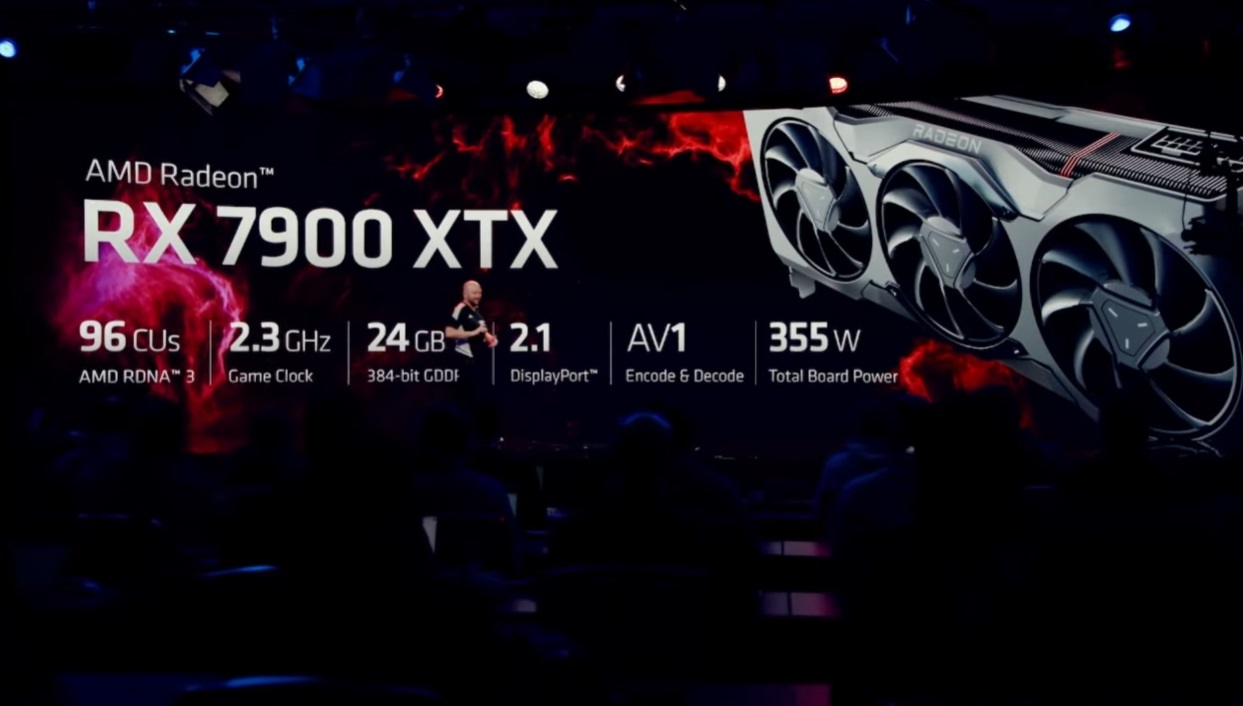
- Navi 31 graphics core with MCD (Multi-chiplet Die) design in a 5nm node for the GPU block and a 6nm node for the cache block.
- 12,288 shaders.
- 384 texturing units.
- 192 raster units.
- GPU at 2.3 GHz-2.5 GHz, normal and turbo mode.
- 61 TFLOPs of power in FP32.
- 96 computing units.
- 96 units for second generation ray tracing acceleration.
- 192 units for AI acceleration.
- 384 bit bus.
- 24 GB of 20 GHz GDDR6 memory with a bandwidth of 960 GB/s.
- 96 MB of infinite cache with a bandwidth of 5.3 TB/s.
- PCIe Gen5 interface.
- 355 Watt TBP, requires two 8-pin power connectors.