As ASML is a company dedicated to the construction of industrial machinery for the manufacture of chips, they have ended up being an authority in terms of knowing how technology will evolve in the following years. Since their units for the EUV have become an essential part in the industry (of which they maintain a monopoly) their future predictions are to take into account, since they are one of the few who can speak with knowledge. of cause on the subject.
ASML: up to 300 billion transistors by 2030
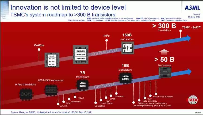
Through an ASML presentation, he has given data on how the chips in our PCs will evolve in complexity for the following years. Of all this, the first thing that stands out is that we will have chips with up to 300,000 million transistors, at least from TSMC as you can see in the slide above. Currently the most complex chip in the foundry in Taiwan is the NVIDIA A100 with a size of more than 800 square millimeters and built under the 7nm node and 54,000 million transistors, which represents a 6-fold jump in density.
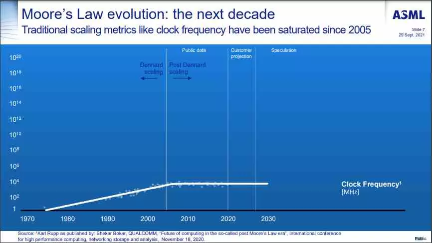
The second point is the clock speed, after the end of the Dennard scaling the clock speed will remain as in the last two decades, in the area of GHz counted by units and therefore not even in 2030 ASML ensures that we will not to see CPU at 10 GHz or more. Nor is it information that has taken us by surprise, since it is many years since the great jumps in clock speed have gone down in history and we have been several generations in which the performance does not come from an increase in this aspect.
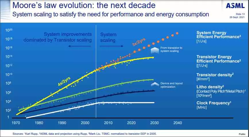
The third and last point has to do with energy consumption. And it is that evolution has not only stagnated in terms of clock speed growth since the Post-Dennard era began in 2005, but we also have to take into account that data transfer grows with the number of cores and the interconnection between them. It is currently the biggest bottleneck and ASML states that the general stagnation will continue until 2030. This confirms a trend that has been taking place in the industry for years, the search for new interconnection systems that allow reducing energy consumption in this regard.
In any case, the prediction in terms of power per watt that has existed since 2005 will remain stable thanks to these new packaging systems such as CoWoS and SoIC by TSMC or Foveros and EMIB by Intel. That is to say, it is speculated that the power per watt could triple every two years, but it must be taken into account that this is taking into account the most efficient architecture together with the most advanced type of packaging at all times designed for the most complex packaging.
Predictions in RAM and NAND Flash
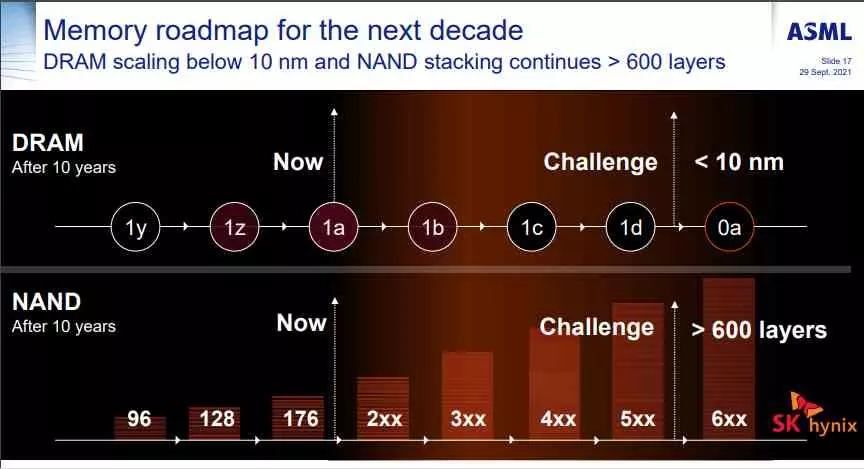
To finish, what we have to highlight from the ASML predictions for 2030 is in reference to the future of DRAM memory. And it is that they predict that we will still see several generations of memory under processes of more than 10 nm, being the current challenge for memory manufacturers to move to smaller nodes. This means that the storage capacity of the system’s volatile memory will not increase much in the following years.
As for NAND Flash, the evolution will be much more aggressive, the challenge is that they end up replacing hard drives and evolutions are expected that will go from the current configurations of less than 200 layers with the future challenge of reaching more than 600 layers. As far as the eye can see, we would be talking about quadrupling to fivefold the storage capacities of SSDs at the same cost.
The future of Intel, Samsung and TSMC is through the use of EUV technology
Given that the EUV is essential for the advancement in semiconductors, from ASML they predict that by 2025 and compared to current figures the number of wafers that will be produced with this technology will double, most of them to build chips of memory.
As for the ASML roadmap, semiconductor manufacturers are currently making use of their EUV 0.33 NA technology, which is used to manufacture chips under nodes between 7 and 2 nm. While for the next generation they already have their EUV 0.55 NA technology ready, of which we know that Intel has been the first large customer to acquire it for their very future node 20A to be the first to have the machinery available and to anticipate TSMC.
In conclusion, the future in processors goes through EUV technology and ASML already has everything necessary for a decade of advances in hardware from TSMC, Intel and Samsung.