Although its greatest novelty is in the AMX unit, which is a Tensor type unit like that of GPUs, but with a difference, while in the case of graphic cards the set of registers is shared and therefore its operation is switched with the SIM units, the AMX is an execution unit by itself that can work at the same time as the rest of the processor, since it has your own set of 1024 records for exclusive use.
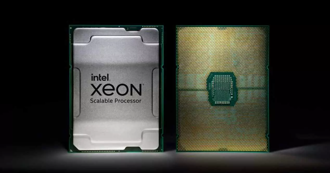
Differences with the Intel Core Gen 12
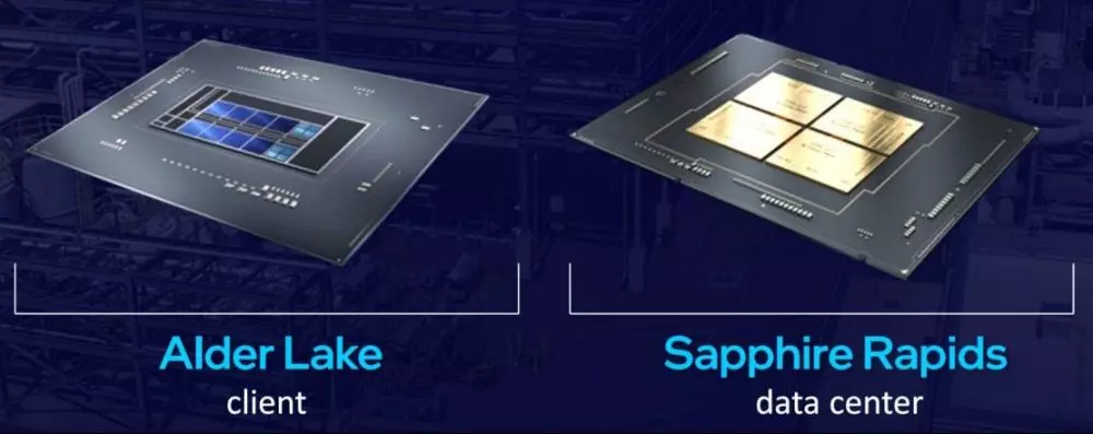
The first thing we have to bear in mind is that the Sapphire Rapids architecture uses a good part of the technologies that have also been implemented in Alder Lake as they have been manufactured under the same node: Intel 7, formerly known as 10 nm SuperFin.
So that share main core, Golden Cove or called P-Core in current company slang. Instead the fourth generation Xeon Scalable Processor does not have Gracemont or E-Core cores inside, but the differences do not end at this point, since it is very possible that we see models with up to 20 cores per tile or 80 per processor.
However, there are important changes in the Sapphire Rapids processors with respect to its counterpart for home computers, the first of which is having the AVX-512 active and the second is the increase of the processor L2 cache from 1.25 to 2 MB. Although the largest is the number of cores that there are in total Sapphire Rapids, since being a CPU designed for servers and data centers it is a beast that makes Alder Lake pale with u
Although the most important change is not in the central processing units, but in an accelerator called Data Streaming Accelerator, which is an IOMMU unit that has been enhanced for use with hypervisors and therefore virtualized operating systems, which makes it designed for cloud computing platforms from the server side.
How fast will the Sapphire Rapids go?
At the moment we do not know the clock speed of each of the Golden Cove cores within each tile in Sapphire Rapids, but we know that it will be lower than in Alder Lake and not because of the fact that they have said it from Intel, but purely knowledge of the subject:
- The AVX-512 instructions have a higher power consumption than the rest, to compensate for this, when executing them, the clock speed is reduced.
- We are facing a server CPU, which in many cases will work 24 hours a day and 7 days a week without interruption, it cannot allow accelerations or operate at high clock speeds.
- It has always happened that if the number of cores of a CPU with the same architecture is increased, the clock speed progressively decreases, this is because it is necessary to reduce the cost of communication.
If we compare with the current Ice Lake-SP based on Cypress Cove we will see that their maximum clock speed is 4.1 GHz, so even with ignorance about the final specification we can assure that it will not be very far since they make use of a process of very similar manufacturing.
Exceeding the limit of the reticle
The title may seem confusing, but you have to bear in mind that when designing a processor there is a limit in terms of its size, which is how large in area it can be. The reason is that the more surface area a chip has, not only less space per wafer making them more expensive, but also the number of errors that can appear is greater. So in the end it is not profitable to make them that size.
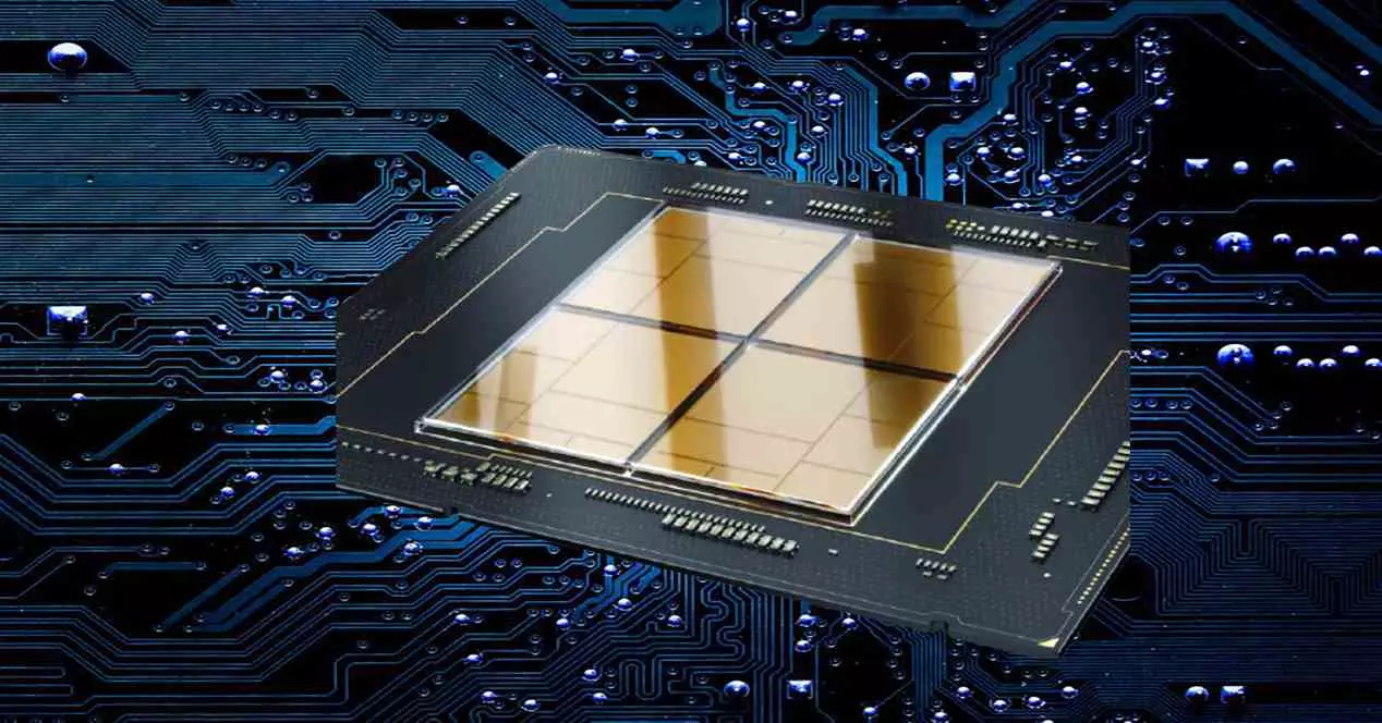
The solution that the industry has come up with is chiplets, which consist of dividing a very large chip into several smaller ones that work as one. The advantage of this is that we can overcome the limit of the grid that we would have with a single chip by using several, which means having in practice the equivalent of a larger processor, with more transistors and therefore with greater complexity.
Of course, here comes the problem of the cost of communication in connectivity. By separating the chips, what we do is increase the wiring distance and with this we end up increasing the energy consumption of communication. Let’s see how Intel has done it in Sapphire Rapids.
EMIB in the new generation Xeons
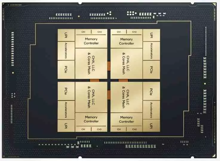
The clearest solution is to shorten the paths, and for this, an interposer is used below, which is a communication structure in charge of communicating vertically with the processors and memories that it has in the upper part. Currently there are two ways to do it, through silicon pathways or idem bridges, being Intel’s EMIB technology of the second type and it is responsible for the four tiles to communicate with each other.
While in the AMD Zen 2 and Zen 3 architecture the last level cache or LLC is in the CCD chiplet, in the case of Sapphire Rapids it is divided between the different tiles. What is special about this cache in every processor? Since the first to the last of the cores make use of the same RAM memory well, the highest level cache is shared by all of them, it is global and not local and therefore each tile in the Sapphire Rapids architecture must have access to the part of the LLC that is in the others at the same speed as you would access your own.
What silicon bridges do is communicate the different parts of the last-level cache that is in each of the tiles in such a way that there is only no additional latency. Also what it does is reduce the energy cost of communication, in the end the effect is the same as having a single chip for practical purposes, but without a size limit in terms of its area.
CXL 1.1 support in Sapphire Rapids
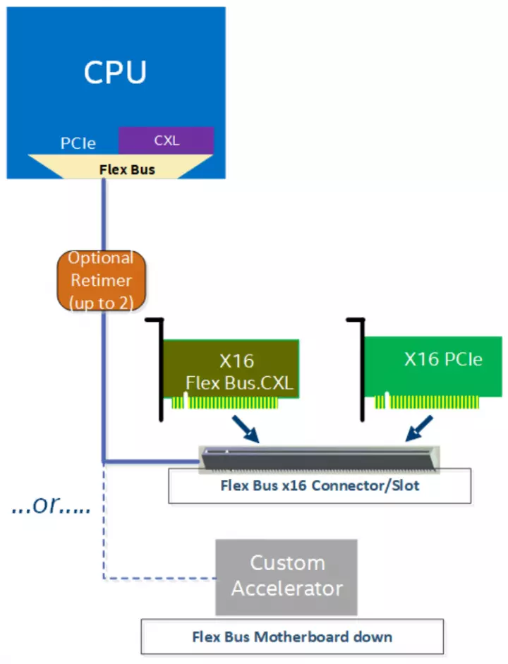
The CXL is going to be one of the most important standards in the next few years, unfortunately Sapphire Rapids does not support the entire standard. And what is this technology about? This is an enhancement over the PCI Express interface that provides cache consistency for processors, memory expansions, and devices. Which makes all of them share the same addressing.
The standard has CXL has three protocols which are CXL-IO, CXL-CACHE and CXL-MEMORY. Its limitation? It does not support the latest protocol and this means that not only coherent PCIe RAM expansions are not supported, but also the HBM2e memory of certain processor models would not be in the same address space, although this would not be the case even with the full support for Compute Express Link since communication with High Bandwidth Memory is done through four additional EMIB bridges, so they do not share the same memory space.