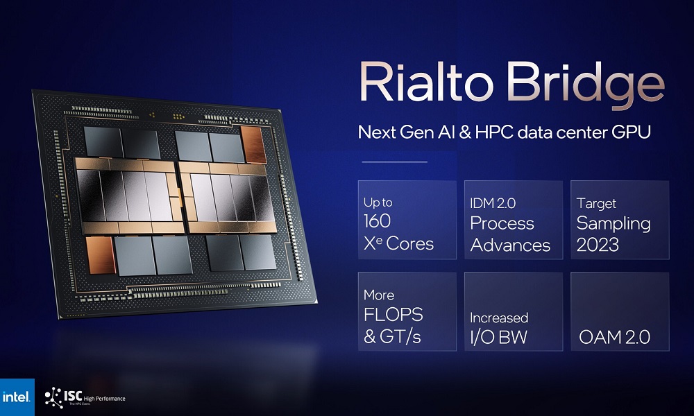
The chip giant took advantage of the International Supercomputing Conference held yesterday in Hamburg, Germany, to present Rialto Bridge, a high-performance graphics accelerator for data centers specialized in AI that uses the same architecture as Ponte Vecchio, although it uses a more advanced node. Nothing has been finalized in this regard yet, but the most logical thing would be for it to be manufactured in the Intel 4 process.
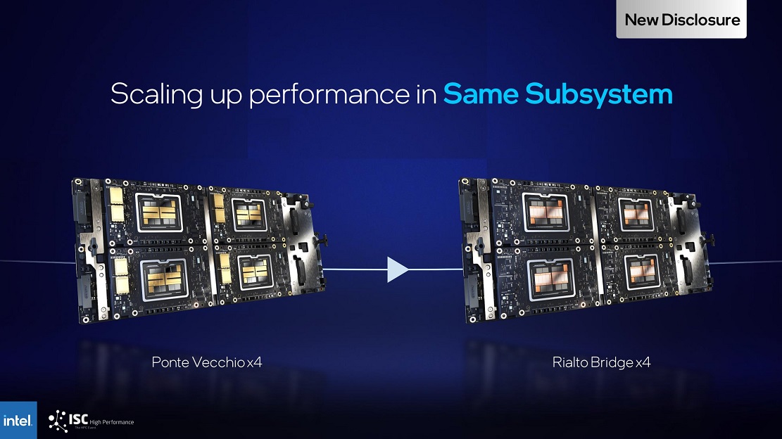
In total, the Intel Rialto Bridge will mount up to 160 Xe cores, which will translate into greater power working with floating point operations, will offer higher bandwidth in input and output operations (I/O) and will have higher limits at the TDP level (up to 800 watts), which will should translate to higher peak raw power compared to previous generations. According to Intel, the first Rialto Bridge units will begin production in 2023, and it will be able to integrate seamlessly into systems that already have a Ponte Vecchio-based setup.
Jeff McVeigh, vice president and general manager of the Supercomputing Group at Intel Corporation, also wanted to highlight the importance of sustainability and energy efficiency on the path that is taking us towards exascale computing, and said:
“As we embark on the era of exascale and move towards zetta scale, the tech industry’s contribution to global carbon emissions is also growing. It has been estimated that by 2030, between 3% and 7%1 of global energy production will be consumed by data centers, with computing infrastructure being one of the main drivers of new electricity use.”
Therefore, Intel has reinforced its commitment to achieve net zero greenhouse gas emissions in its global operations by 2040, and is also committed to developing more sustainable technology solutions.
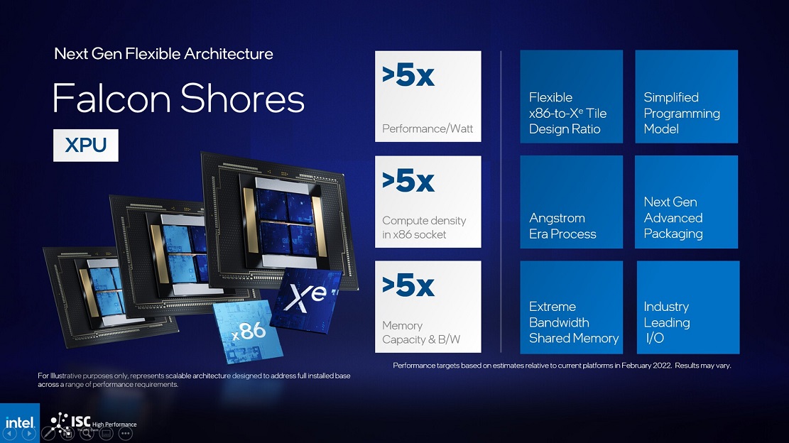
In another order of things, Intel has also presented the XPU Falcon Shoresa flexible and scalable solution that marks an important innovation at the architecture level according to the chip giant, and that will join the x86 (CPU) and Xe (GPU) architectures in a single socket. It is a project planned for 2024 that promises to multiply by five the performance per watt, the computing density in the x86 socket and the capacity of memory and bandwidth, all in a new generation package.
In case someone is lost, I remind you that an XPU is defined as a complete cross-architecture computing solution that normally includes all major types of chipsinterconnected and united under a single application programming interface (OneApi in the case of Intel Falcon Shores) that it assigns each task to the chip that can best handle it. In other words, the XPU represents a huge step forward on the path to integrated heterogeneous computing, and it obviously relies on an MCM (multi-chip module) design.