In a presentation, Intel has revealed its Roadmap of processors and manufacturing nodes with important news regarding the future of the company currently led by Pat Gelsinger. The new information that Intel has provided gives us a much clearer roadmap regarding its plans to compete against AMD in the CPU market and against TSMC when it comes to third-party manufacturing.
Intel renames its manufacturing nodes
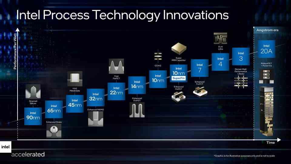
In a marketing strategy, but with all the sense in the world. Intel has renamed its manufacturing nodes, since until now the fact that its 10 nm node was equivalent to that of 7 nm from TSMC and better even than its biggest rival in semiconductor manufacturing.
The fact of telling the general public that a 10 nm node is equivalent to a 7 nm node, as it was confusing to say the least, so Intel has decided to rename its 10 nm node, whose next version received until now the name of 10 nm made SuperFin with the simple name of Intel 7, which is already in production in high volumes as it is the node to be used by Alder Lake and Sapphire Rapids. The advantages over the 10nm SuperFin node used in Tiger Lake-H? Between 10% and 15% yield.
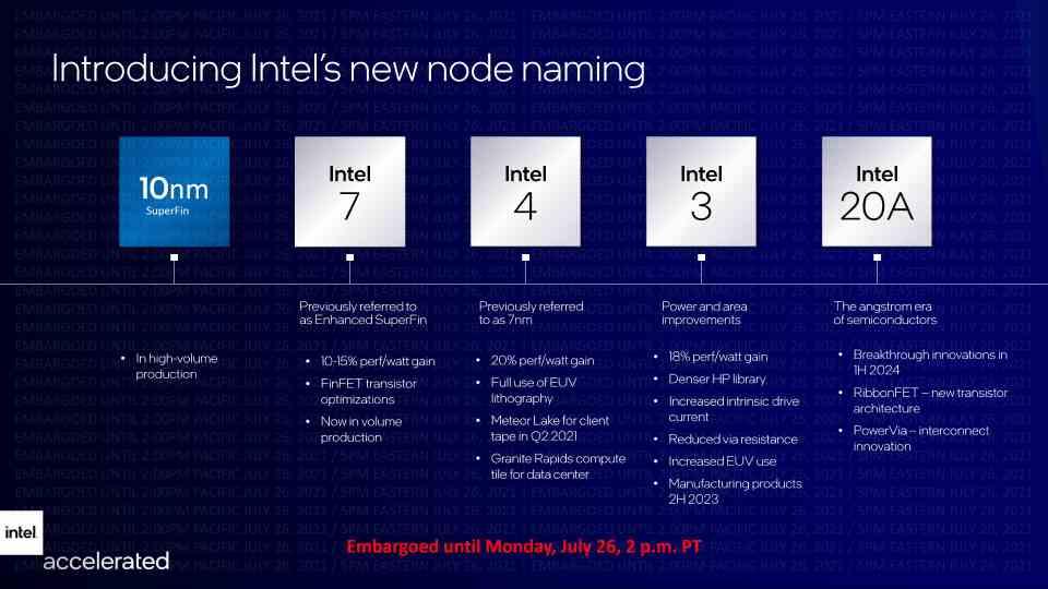
As for the future of the node formerly known as Intel 7nm, equivalent to the 5nm node in terms of specifications and density, this has been renamed to Intel 4. The improvements over Intel 7? Well they have promised a Additional 20% as far as performance per watt is concerned. The manufacturing node Intel 4 will be used in Meteor Lake and Granite Rapids, being the first of Intel to make use of EUV lithograph. Its release date? Intel has already completed the end of the process to design the Compute Tile what form of these processors in the second quarter of 2021, so it is expected that chips will begin in 2022.
The third node is dated 2023, it is about Intel 3 and it promises another 20% increase in performance over consumption compared to its predecessor. With all this, we can deduce that Intel intends to introduce a new manufacturing node every year, a feat at least difficult.
After the nanometers come the Armstrongs
Intel has not only talked about the commercial renaming of its manufacturing nodes that we already knew in advance, but also about the manufacturing nodes that will come next, and again it seems that we have an almost annual cadence
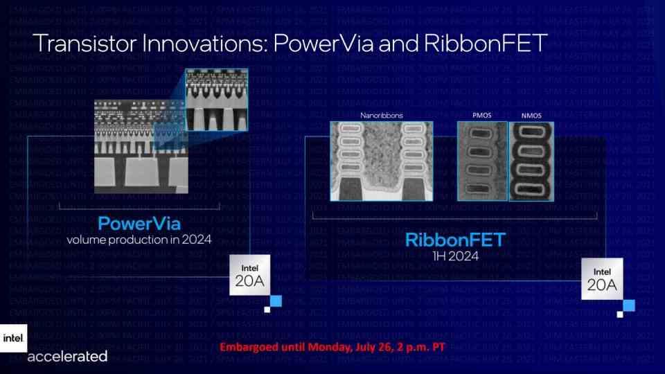
For 2024 Intel has planned a new manufacturing node, which they have dubbed as Intel 20A, where the A refers to Armstrong, which is a measurement where a Armstrong has the size of 0.1 nm. From what we can deduce that it could have been called Intel 2. The differences with other nodes? Intel will introduce a new type of transistor dubbed RibbonFET, which are Intel’s implementation of the Gate-All-Around Field-Effect Transistor or better known as GAAFET.
The second novelty is called PowerVia , name that refers to the new PDN that Intel will introduce in node 20A, and therefore of a new way of supplying energy. The novelty is that all the interconnections for the PDN in the upper part of the chip will be moved to the lower part of it, from where they are directly connected to the chip without going through the interconnection interface.. Which would have to go through the PDN if it were on top of the chip. All of this could mean that the Power Delivery Network of the processors under the Intel 20A node would be on a separate chip in a 3DIC configuration.
But the thing does not end there and despite the fact that Intel has not included it on the road map. have talked about another manufacturing node, called Intel 18A, which would be planned for early 2025 by making improved RibbonFET transistors. What is unique about this manufacturing node? It requires a new type of machinery for lithography by making use of the High NA EUV, a type of high precision EUV machinery from ASML that is necessary for such a small manufacturing node. Intel will be the first foundry in the world to receive this type of machinery.
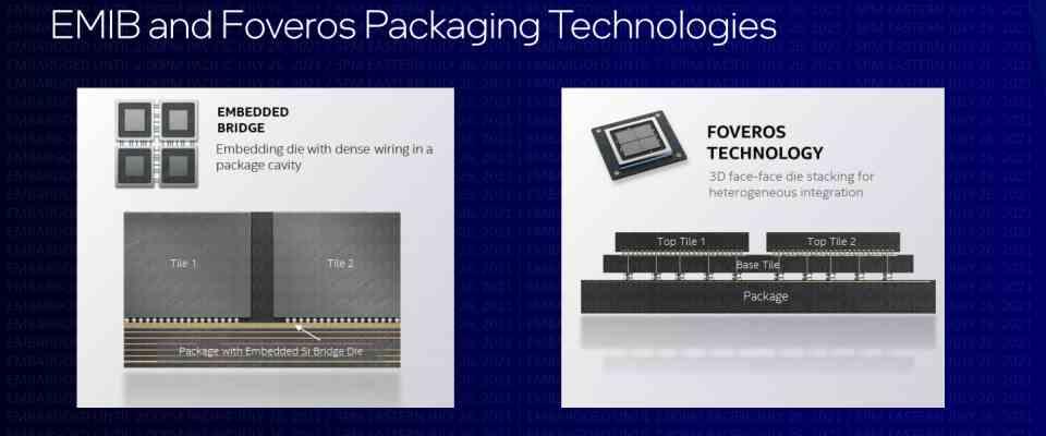
New 2.5DIC and 3DIC packaging technologies
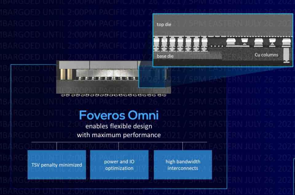
Intel has introduced two new flavors of its 3DIC packaging, generically christened Foveros.
Being the first of those that Intel has presented Omni Foveros, which is an evolution of the Intel Foveros technology used in Lakefield processors. It is a 3DIC packaging system that allows direct interconnection between the two chips. Foveros Omni allows a single processor to be broken up into several different chips with different manufacturing nodes each. Intel expects Foveros Omni to be ready for mass manufacturing by 2023.
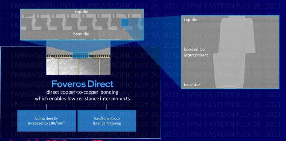 Foveros Direct On the other hand, it is another flavor of Foveros, but it is designed for direct copper-copper connection. One of the reasons why the vertical interconnection between chips or 3DIC exists is to increase the number of interconnections, which allows increasing the bandwidth without having to shoot the clock speed north, thereby causing high consumption. This is achieved by making use of matrix interconnections instead of serial, so the size of these interconnections is important.
Evolutionarily Foveros in its first generation for Lakefield makes use of interconnects 55 micrometers in size, but the second generation of Foveros that we will see in the HPC Ponte Vecchio GPU decreases the size to 36 micrometers. The size of Foveros Omni and Foveros Direct? 25 microns and less than 10 microns respectively. They have also revealed that both Foveros Omni and Foveros Direct are not only combinable with each other, but also with Intel EMIB to create complex heterogeneous systems.
The next generation of Intel processors in the new nodes

Intel has not only talked about its new packaging and its new manufacturing nodes, but also about the processors that we are going to see at least in the next three years, both at the PC and server level. Being the first those that will use the Intel 7 node and therefore Alder Lake and Sapphire Rapids. Of which we already know enough details and whose design, at least in the case of Alder Lake, is fully completed.

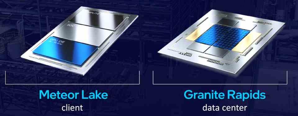
But where Intel has shown more news is with Meteor Lake, which is a chiplet-based design where intercommunication is done using several interconnected tiles using second-generation Foveros. Meteor Lake will use three different tiles, the first is the Compute Tile, the second is in charge of the processor I / O and the third is an Intel Xe GPU that ranges from 96 EU to 192 EUs.
All the tiles in both Meteor Lake and Granite Rapids are connected to what Intel calls the Base Die at the bottom. Which will be in charge of the different intercommunication between the nuclei making use of the second generation Foveros interconnection. This is the same intercom technique that Intel uses on its Intel Xe-HPC or Ponte Vecchio GPU.