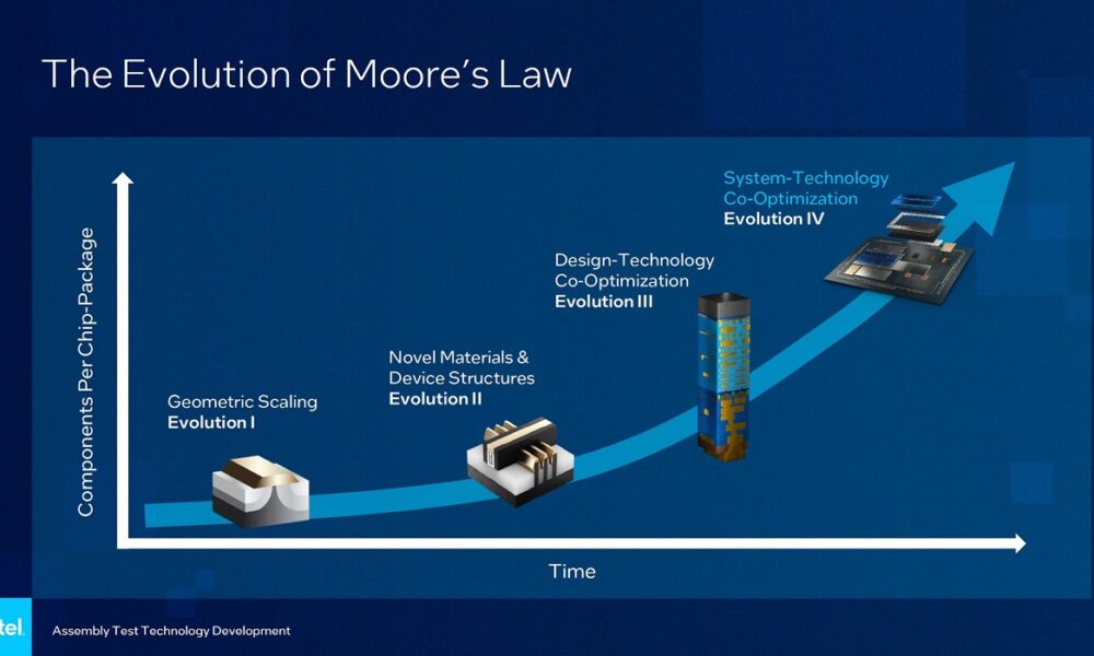
A few days ago we had the opportunity to attend an event where Intel showed us the evolution that the company has experienced at the chip packaging level. This allowed us remember the most important jumps that have occurred in this regard in recent decades, something that gave us the perspective we needed to better understand all the advances that have allowed us to get to where we are today.
Intel made a simplified division to make it easier to differentiate a first stage of packaging, which we can consider as the oldest, and the advanced stage, which is where we are today. In that ancient stage groups, for example, the packaging used by processors as mythical as the 8086the ceramic packaging of the mythical Pentium and also the multichip packaging of other more current processors, such as the Core 2 Duo, for example.
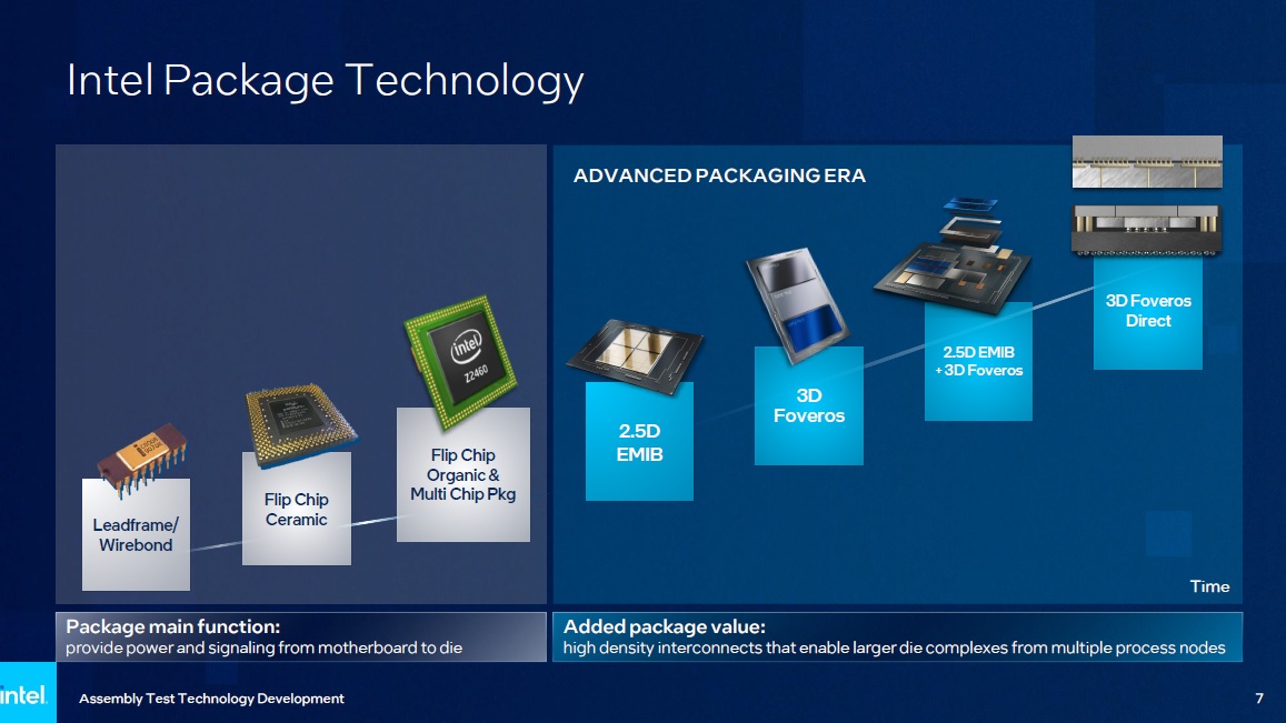
At that early stage, one of the main purposes of packaging was supply power and signal from the motherboard to the package. The leap to advanced packaging has been implemented in solutions such as Sapphire Rapids, which introduced a 2.5D EMIB design at the silicon level. Also noteworthy in this regard is the Foveros technology, which allows stack chips in 3D and implement different blocks to create a complete system in a single package, and that, as we see in the image, will continue to advance thanks to the EMIB 2.5D (acronym for Embedded Multi-die Interconnect Bridge).
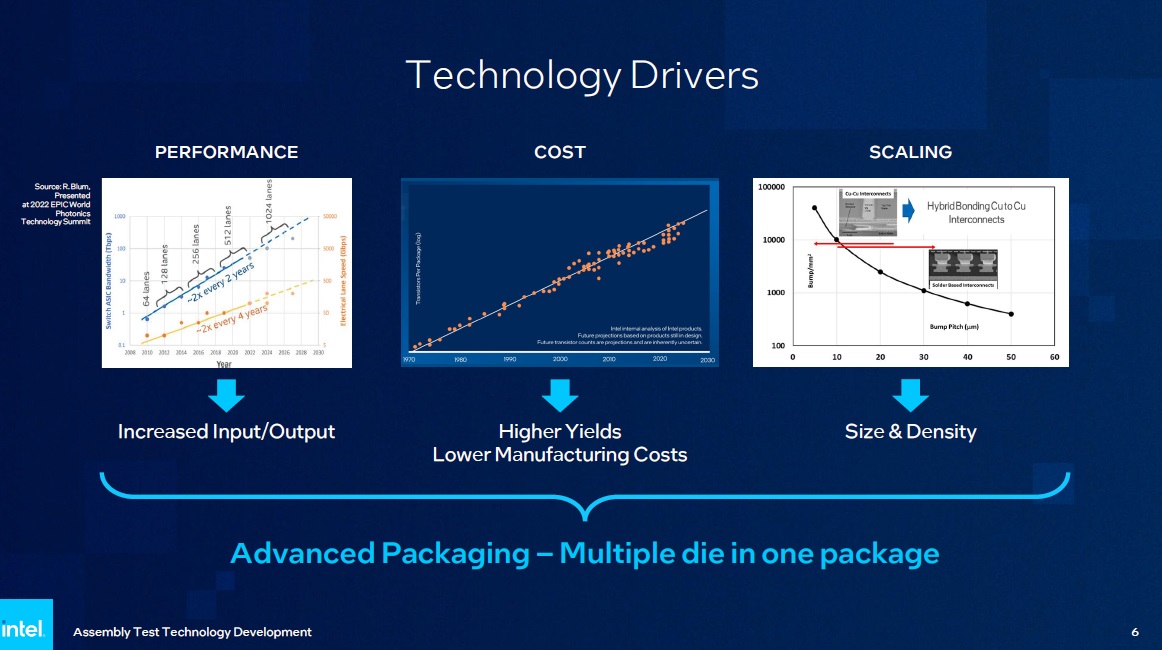
At that stage of advanced packaging it is possible to create multi-chip systems in a single package, thanks to chip stacking and the use of interconnect bridges multi-encapsulation bridge. This opens the door to new larger designs with higher transistor densities, allows chips from different processes to be used in the same system in a single package, and significantly reduces manufacturing costs by minimizing the complexity of moving them to the wafer. Also lowers production costs.
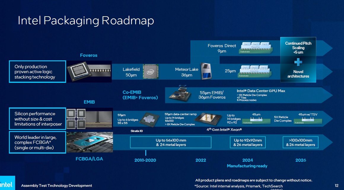
In this event it became clear that Intel has known how to play its cards when it comes to betting on the stacking of 3D chips, and also on the interconnection of 2.5D packages, thanks to the EMIB system. We were also able to see a very interesting roadmap where we found the most important goals that Intel has set in this regard for 2026, and which you can see in the attached image.
On this subject, one of the developments that most caught my attention was, without a doubt, the future jump to a next generation interconnect system based on co-packaged optics made of glass, and equipped with integrated waveguides. In theory, they will further improve the success rate and reduce manufacturing costs. The latter is precisely one of the key points for which Intel is transitioning from the monolithic package design to a 3D stacked multi-chip and multi-system packaging design, production costs.