The biggest challenge in a system made up of several different processors is communication. However, there are applications where the power required by the hardware prevents placing the architecture on a single chip and a more complex composition has to be drawn, the most common being what we call a 2.5DIC circuit.
The problem with silicon interposers
Due to the complexity of the necessary communication and the need to save on data transfer, the use of complex communication interfaces is required. The most common trick? The use of vertically placed silicon pathways that run from the interposer and through the chips vertically. This allows you to increase the number of interconnects and make each one go at a low clock speed, which is extremely important since power consumption grows exponentially with clock speed.
The problem with silicon interposers is that they are extremely expensive Due to the size of the interposer, since this is really nothing more than a chip on which the rest of the chips are mounted and it must also be large. So the size of the interposer is limited by the manufacturing node grid. With current technology, the maximum size that a silicon interposer can have is 30 x 30 mm, so the chips, both memory and processors, must therefore be smaller than the interposer on which they are mounted. .
All these limitations mean that for a couple of years an alternative has been developed in the form of the so-called silicon bridges, which have been adopted by both Intel and AMD for their present and future 2.5DIC designs.
What are silicon bridges?
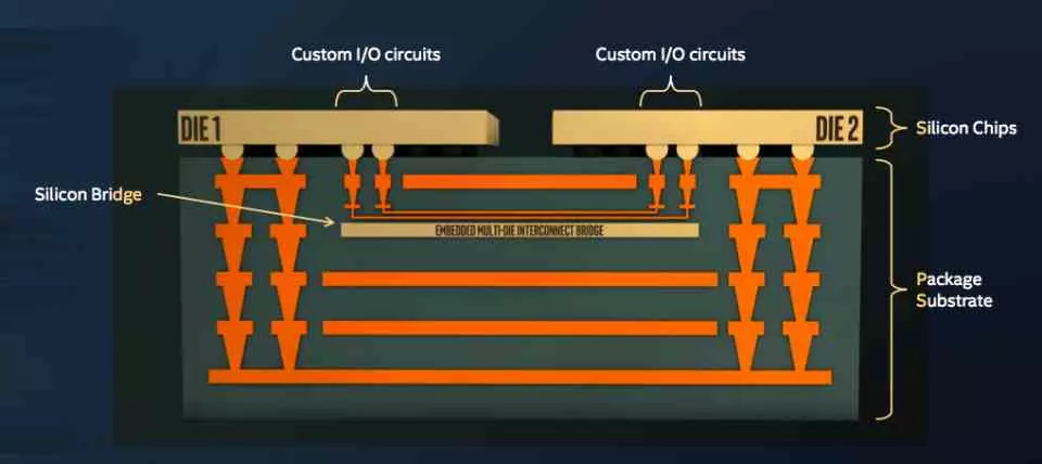
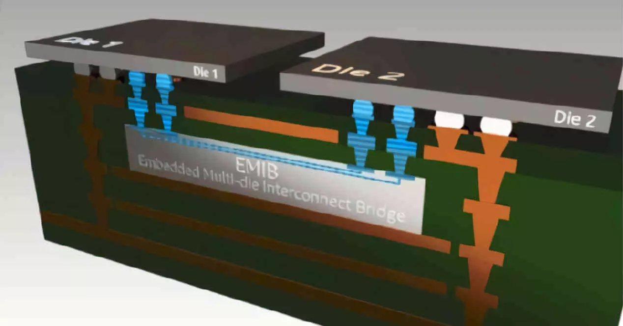
Silicon bridges, silicon bridges in English, they are not a future technology, since we have already seen them in products that have been released on the market. Since EMIB technology and Intel use this technology to communicate various chips with each other in their designs based on two and a half dimensions integrated circuits.
The advantage of silicon bridges is that they do not use a whole interposer for communicationInstead, they create a communication channel between the two chips that are in communication that is located on the substrate of both chips. Something that at first glance may seem like an interposer, but really the amount of silicon needed for the intercommunication of the different chips it is much smaller.
In addition, silicon bridges allow freedom when joining different chips together, creators are not limited by the size of the interposer and there is no interconnection overhead in the interposer that then there are elements that they do not use to communicate. each. It is therefore a much cheaper solution and brings 2.5DIC designs closer to the home market and therefore outside of high performance computing.
How do silicon bridges work?
One of the peculiarities of silicon bridges is that do not make use of pathways through silicon or TSV to intercommunicate with the chips, which greatly reduces costs, since there is no need to create a series of vertical pathways that traverses the entire chip from top to bottom. The problem with adopting silicon pathways is that it is as complex as building a building. And once it is built, say that you have to run a network of pipes through the middle, which technically means having to drop the building to the ground and do it again.
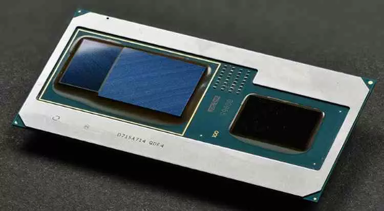
As with the TSV of the silicon interposers, the silicon bridges also intercommunicate vertically, but this intercommunication is done on a bridge that is between both chips and gives enough bandwidth for communication. For example Intel with the launch of its first generation EMIB technology was able to communicate an AMD GPU with its HBM memory using one of the silicon bridges in Kaby Lake-G.
Who is adopting it?
Both Intel and AMD are embracing silicon bridges in the development of future products, although as we have already mentioned, Intel has already adopted them and specifically it was in a joint project with AMD. We are referring to the NUC Hades Canyon and the way in which CPU and GPU were interconnected with each other via a silicon bridge.
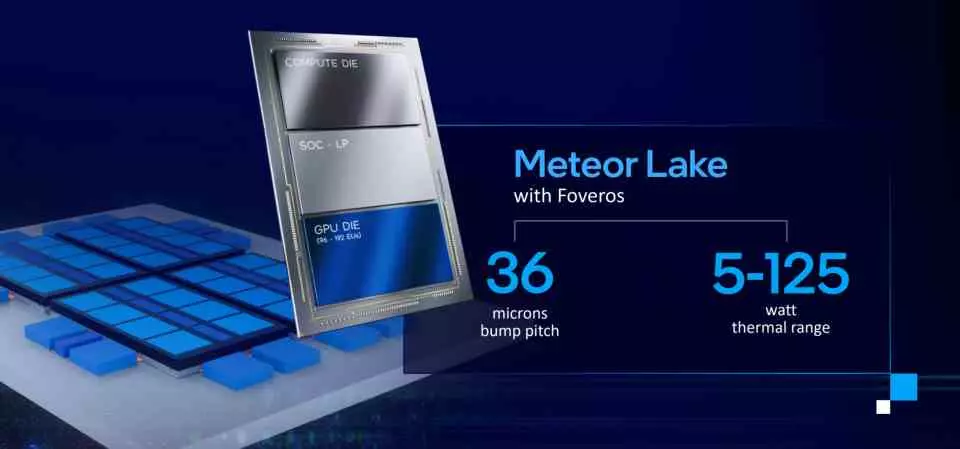
The product was not very successful, but Intel has developed their silicon bridge technology, EMIB, during all this time and has turned it into the way to interconnect the different tiles, which is what they call chiplets, in designs both the not yet released Intel Xe-HP GPU, as well as the future Intel Meteor Lake CPU. Which we hope will be on the market by 2023.
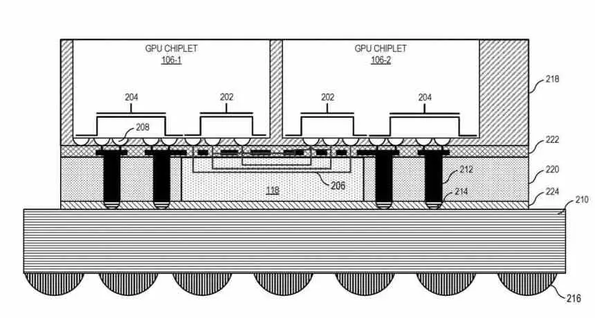
In the case of AMD, on the other hand, the adoption of silicon bridges we will see it in RDNA 3, whose reference we have thanks to a series of AMD patents where they describe a Gaming GPU composed of several GPU chiplets. Which are seen by the operating system as if they were a single GPU. Interestingly, for the range of CDNA 2-based MCM GPUs, AMD uses a common interposer, but it should be noted that the high-performance computing market has costs that can be borne by TSV and the use of silicon interposers.
In general, it is expected that in the coming years silicon bridges will be adopted by different manufacturers who want to build 2.5DIC solutions for the domestic market, something that we have been waiting for years and that will be one of the elements that will solve the problem of the rise in costs for the end of Moore’s Law. But, for the moment and to finish, we are left with the following: it is not an unproven technology and therefore we are not talking about something science fiction.