The HBM3 memory still does not have the definitive standard, but designers from different parts of the world have their proposals ready, since whoever manages to make their proposal a standard will have the benefit of being the first manufacturer to power the first GPUs for high-end computing. performance. So despite the fact that there is still a long time to go for the new generations of NVIDIA Tesla and AMD Instinct with this type of memory to reach the market, time runs against it, since the interfaces with the new types of memory have to be developed. .
In the case of memories of this type, the complication increases if we take into account that both the GPU and the memory are mounted on the same interposer, which will have different specifications in the HBM3 than in the current HBM2 and not only includes the routing between the memory and the graphics chip, but the entire Power Delivery Network in charge of distributing the energy between the different elements on top of the interposer.
This is the HBM3 memory according to SK Hynix
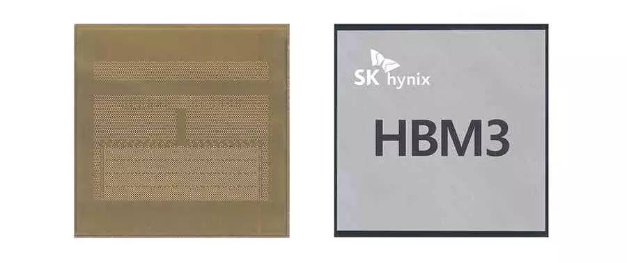
Currently South Korea is the largest manufacturer of memory, both non-volatile and RAM, in the world with specialized multinationals such as Samsung and the one that concerns us in this news. And it is that SK Hynix has presented its prototype of memory HBM3 and therefore its proposal in order to be accepted by the JEDEC. The advantage over the rest? Well, by having their own foundry they can manufacture the memory and go beyond a design in VHDL or Verilog.
And what have they achieved? They have manufactured two different batteries, the first composed of 8 memory chips and 16 GB capacity in total and the second with a stack of 12 and 24 GB capacity. So it is the first time that we see the limit of 8 chips per stack being exceeded in a memory of this type.
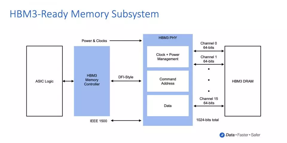
Regarding the bandwidth, they have reached 819 GB / s, we must bear in mind that the point where HBM3 memory differs from its predecessors is in the use of 64-bit memory channels per chip in the stack instead of 128 bits. This means that in a 1024-bit interface we can put up to 16 different chips. A 12-chip stack is a 768-bit bus and a bandwidth per data pin of 8.5 Gbps, although it is possible that the transfer speed that SK Hynix talks about is with the 1024-bit bus.
If this were so, then we would be talking about a real bandwidth of 409.6 GB / s in the case of the 8-chip stack and 614.25 GB / s for 12. In both cases we would be talking about 6.4 Gbps per data pin.
The size of the interposer is crucial
The HBM3 memory appears to have taller and smaller chips than previous generations of the High Bandwidth Memory standard, but in its HBM3 SK prototype, Hynix has reduced the height of the DRAM chips. 30% Compared to the previous generation, we must not ignore the use of more advanced manufacturing nodes.
The reason for using 64-bit memory channels and thus having smaller chips has to do with the fact that interposers are giant monolithic chips on which both CPUs and GPUs that make use of this type of memory will go and therefore space is limited. If we add to this the use of chiplet-based GPUs then the area becomes a precious commodity. In other words, smaller HBM3 chips like those from SK Hynix give more headroom to the CPUs and GPUs of the future.