In the chip foundries of TSMC, Samsung and Intel the EUV machinery of ASML is common, since the job of these means of production is to laser engrave the wafers to create the chips under the most advanced nodes. To do this, logically each one makes use of a laser with a power of several hundred watts, which are fired before a complex group of mirrors that allow the content of the wafers to be molded. In other words, this light is used to mold the chips that end up in our electronic devices.
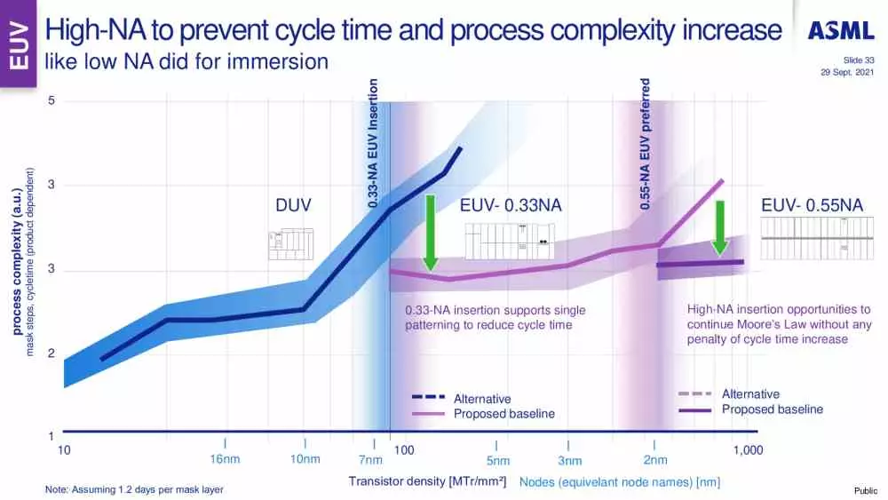
What we know is that ASML will make the leap to a new type of EUV – NA machinery in the coming years and with greater precision, however such technology has a limit and the dependence of the machinery sector on ASML is something that powerfully calls the attention. To the point that a simple ban on the distribution of such production systems to certain foundries in China has completely closed their progress.
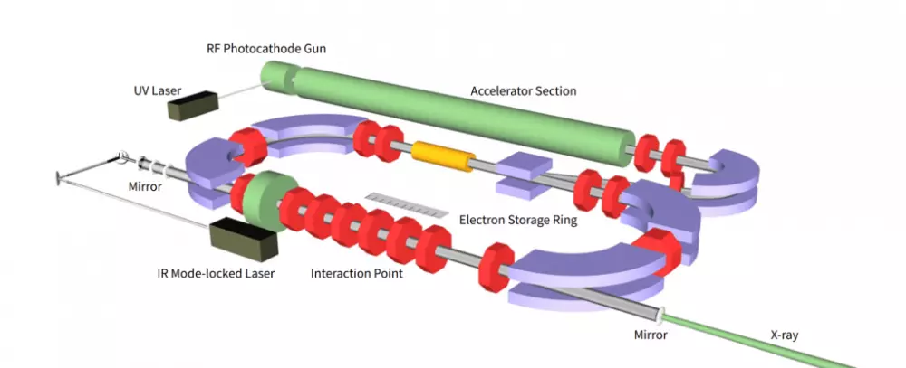
That is why the development of alternatives to the ASML machinery to model the wafers in the chips of tomorrow is one of the fields that is most investigated and at the moment it is the use of particle accelerators at scale that seem to have more numbers. in being the future in hardware construction.
The synchrotron, the alternative to ASML’s EUV machinery
According to sources with knowledge on the subject, the situation with EUV machinery in manufacturing nodes such as TSMC’s 3 nm is such that 10 EUV machines achieve a production speed of 15,000 wafers per month. This translates to 500 wafers per day for the 10 machines and 50 per day per machine. This being the bottleneck for the production of new chips.
For example, the Taiwanese foundry has a capacity close to 150,000 wafers per month with the current manufacturing nodes (without EUV, only DUV), which means that under its N3 node, maintaining said production would need an average of 100 units of ASML EUV scanners. . And we must assume that this is enormous energy consumption, especially in an environment where climate change has become the most complex political and environmental issue for development in the coming years. To give you an idea, there is talk of consumption of 500 W for each of these machines. We have talked about 100 machines, right? Now imagine a chip manufacturing plant in which only the part of printing the wafers has a consumption of 50 kW.
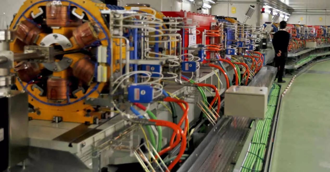
The alternative passes around the Synchrotron, a miniature private accelerator that makes use of magnets that allow it to manipulate electrons and thereby generate photons. Despite this method, despite the fact that it seems to scale much better in terms of consumption and allows creating means for smaller size production, and therefore being better on paper, it has not yet resolved the ability to collect light efficiently. so that it can be used as a substitute for ASML machinery in creating new chips.