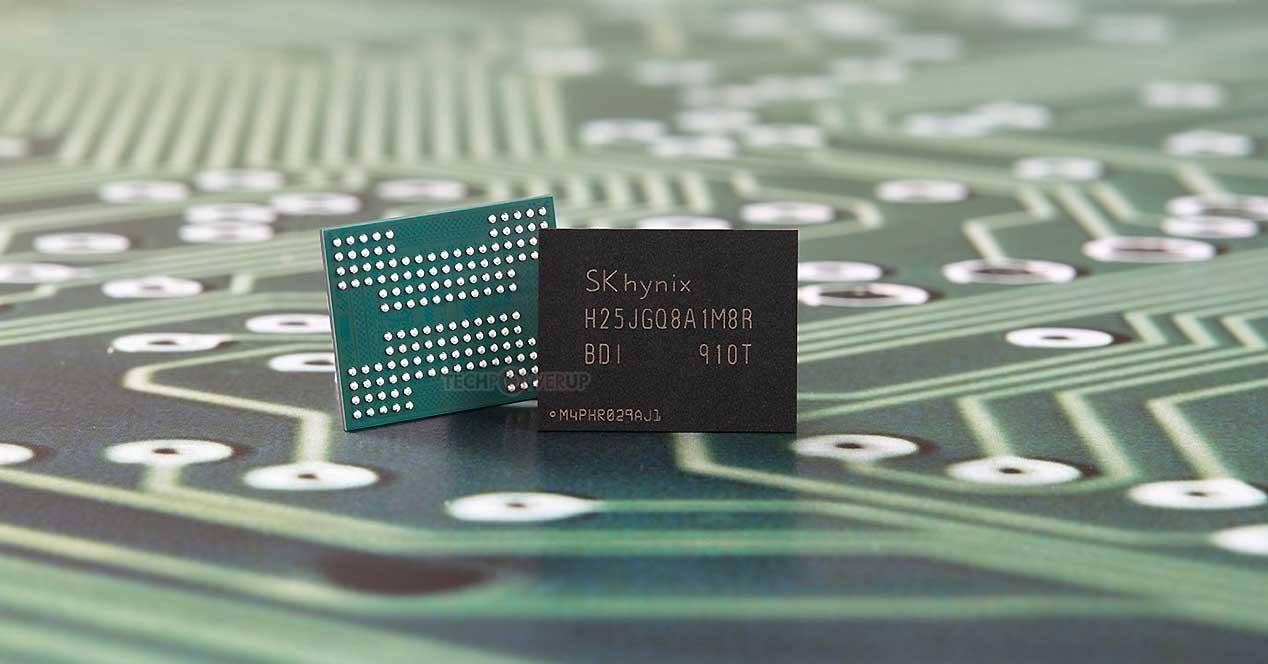
The first 3D NAND chip was launched in 2013, it was Samsung’s first V-NAND with 16 GB capacity and composed of 24 layers. Over time, the number of layers has evolved and today we can find 176-layer 3D NAND configurations. Is there a limit to the number of layers in 3D NAND?
What is NAND Flash memory?
NAND Flash memory is a type of non-volatile RAM, this means that it maintains its information after having lost power. Like RAM, it is organized by memory chips, but unlike RAM it has lower bandwidth and higher latency.
It is therefore a storage memory that is used like hard drives, which, like RAM, grows year after year thanks to the effects of Moore’s Law. Something that is accelerated by the deployment of 3D NAND memory. Which uses dozens of stacked 2D memory chips, making the storage capacity several times that of RAM.
Why is 3D NAND necessary?
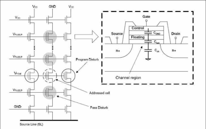
The main difference between classic 2D NAND memory and 3D NAND memory is the way the cells communicate. In 2D NAND the memory cells where the bits are stored are found together with each other on a single chip. So the capacity of each chip is determined on the one hand by the type of cell used and on the other by the number of cells that we can fit on a chip.
For these reasons 2D NAND is limited by two factors. The first of these is the best known and has to do with the capabilities of the manufacturing node that is used to manufacture memory. That is, the number of transistors per mm2. On the other hand, the second reason is more unknown, since it has to do with the reduction of the distance between the transistors and the electric fields that are created.
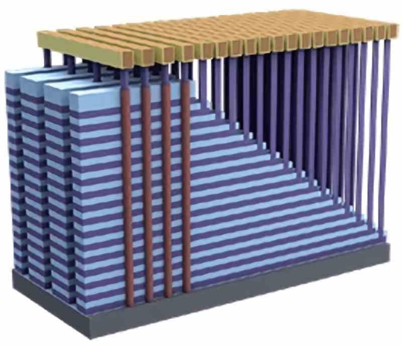
In other words, the closer the cells are, the more danger there is that the electrical charge of a cell ends up corrupting the data of a neighboring cell. Hence the need to implement 3D NAND systems that is based on intercommunicating several 2D NAND chips vertically. The idea is to decrease the density in terms of cells in each of the chips in the battery to prevent the electrical charge of one of the cells from destroying the content of the others.
It is precisely this fact that makes the 2D NAND chips used to build the 3D NAND from a less advanced manufacturing node and therefore with lower density in terms of the number of transistors than those that are purely in two dimensions.
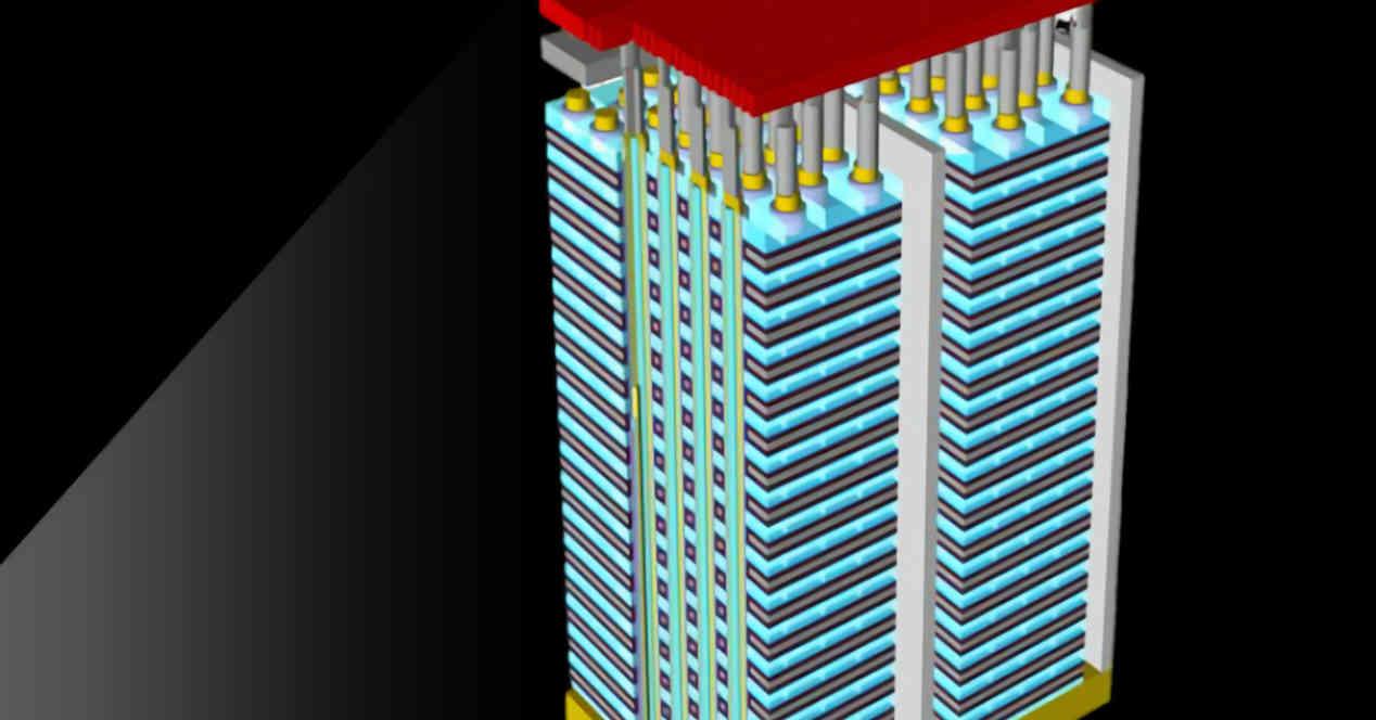
How many layers does 3D NAND memory support?
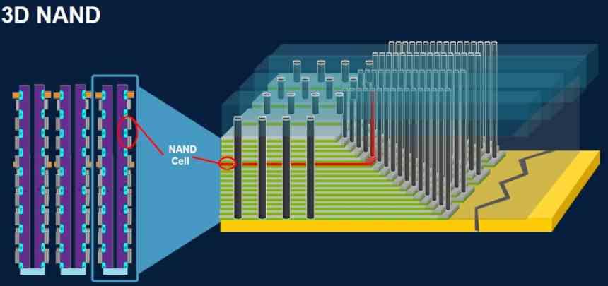
3D NAND memory, however, differs from 3D RAM like HBM by the way the memory stack is organized, since starting with the memory chip at the base of the stack, the rest of the chips that are placed on top are smaller in size, until the point is reached where the 2D NAND memory chips that make up the stack are too small to scale further. It must be taken into account as we have explained in the previous section that the use of new nodes and the increase in the density of the cells forces certain levels of storage capacity to increase the number of layers in order to avoid contamination. electrical power between cells.
On average, manufacturers are adding between 30% and 50% more layers with each generation of 3D NAND. Currently, 96-layer 3D NAND memories are the best sellers with more than half of the market share, followed by 128-layer ones with 15% of the market share. Generational evolution? On average every 18 months, so it will not be until the end of 2022 that we will see the next generation of 3D NAND memory with 256 layers.
Increased capacity thanks to QLC and PLC cells
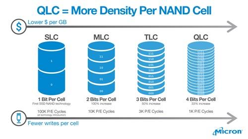
PLC cells are the least reliable of all, allowing up to 4 bits per cell to be stored but limiting the life cycle of the products. However, the need for storage capacity for many people has increased the demand for QLC cells, which in 2021 have been 15% of the demand, but it is expected to reach 50% of it by 2025.
The process is expected to be repeated with the 5-bit cells or PLC that Intel submitted as a proposal a few months ago. At the end of the day it is the same process that has already occurred with TLC and later with QLC. Although the predictions are made from the use of QLC cells and technological advances for 2025.
In what situation will we be? By 2025 we are expected to reach the cost of 2 cents per Gigabyte of storage. Which translates into a cost reduction of 20% year-on-year on average and therefore 30% between generations. By 2025 we should expect 3D NAND configurations with 384 layers.
When will 3D NAND replace hard drives?
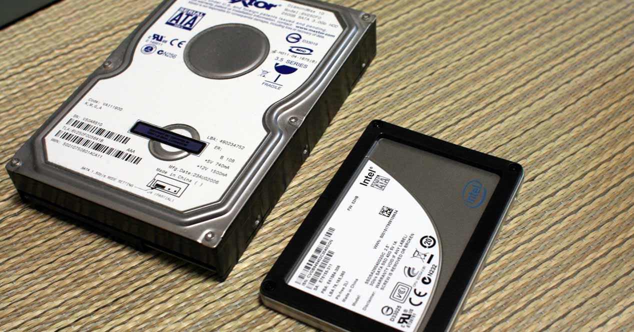
Conventional hard drives are superior to NAND Flash memory in one thing, their ability to store data. It is true that we can draw a list of things in which SSD units are superior at the moment, such as the fact that they do not depend on mechanical parts, have faster search times and above all a greater bandwidth.
The question is: in what year will the cost of 3D NAND be as cheap as a hard drive? Well the predictions point to 2033, so there is still more than a decade for hard drives to be outmatched in what they exceed 3D NAND memory.
The reason why we are going to have to wait so long is that the cost of the manufacturing nodes that are going to be deployed in the following years are going to be more and more expensive, which is going to be a factor in that aspect. However, this does not mean that we will continue to use hard drives for years to come, especially since SSDs are increasingly popular and have advantages beyond storage capacity.