NVIDIA is currently immersed in a legal process to be able to register the Hopper architecture as its own, since another company uses that name for its products. If this is already a stumbling block in the road, what we are going to see next is no less, since it suggests quite a few problems that we understand have been secretly solved.
Here again you have to play not with what is said, but with what is not told. The first Leaker reported on the fact that the GH100 chip (top of the range Hopper architecture) would have more or less an approximate area of 1,000mm2. This in itself is an impressive number considering that GA100 barely exceeds 800 mm2 (826mm2 to be exact) and is fabricated at 7 nm.
These are 858mm² (26*33) and 980mm² (35*28), ~<50% yields not counting redundant structures seems a bit too much for me.
Unless this is a flagship of flagships sold 20k$ a piece to HPC customers. This almost seems more profitable to just take one entire wafer to go. pic.twitter.com/2Fh1twbaqr
— Rule110 (@Rule1103) January 29, 2022
GH100, on the other hand, will reach 5 nm and it is speculated with a size of over 858 mm2, since the size of the wafers is still 300 mm and the number of chips would be more optimal in terms of profitability for each one recorded, since from those 858 mm2 (33 x 26 mm per chip) 26 good days would come out, while if we increase the area to 35x28mm (980mm2) fewer useful chips are wasted, but it results in 5 good dies, with NVIDIA either losing a lot of money per wafer, or else making the chips at a much higher price.
GH100: monolithic architecture or just a monolithic chip
GH100 does not have MCM, it’s still monolithic.
— Greymon55 (@greymon55) January 29, 2022
Here the differences lie in the concept and in the information given. The Leaker’s Response greymon55 to Kopite7kimi It is quite interesting, since it does not refute the approximate measurements of the die, but rather supports the idea of a single die in the so-called GH100, therefore, it is not a dual MCM package as speculated, it would still be a traditional monolithic chip.
Why is that important? Until now, the leaks told us that Ada Lovelace was NVIDIA’s monolithic architecture for gaming, while Hopper would go for data centers, IA and DL as an MCM chip in the purest AMD style with Ryzen (saving distances). With this confirmation, the idea is ruled out and the changes could be minor in terms of chip design, leaving AMD alone with RDNA 3 in this section.
DO NOT overreact. We know the actual die size will be significantly smaller than the package size.
But GH100>GA100 is confirmed. 😁— kopite7kimi (@kopite7kimi) January 29, 2022
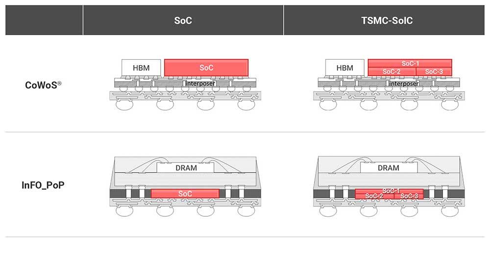
There is also the possibility that NVIDIA will launch a new series of chips that are MCM and so we are not approaching all this in the right way. We must emphasize that there is talk of a specific chip (GH100) that until now and according to the nomenclatures should be the best of the brand for architecture, but nothing tells us that it does not launch a new and separate series of chips with MCM designs per package, where HBM3 and newer substrates are used TSMC 3D SoIC.
Little by little, data is being confirmed, but we are very far from being able to see the complete picture, so be patient, the information will come.