Several years have passed since AMD released its first Ryzen 1000 processors based on its first-generation Zen architecture. Which was a change of luck for the company led by Lisa Su and that AMD will no longer be seen as a brand of cheap CPUs always in tow from Intel. Today, AMD architectures can not only trade blows with Intel’s, but also surpass them in several respects.
In the case of Zen 3, it has assumed that the AMD tortoise has overtaken the Intel hare. Which has realized the danger of an AMD that has cut market share in x86 processors in the different segments of the same in which they compete from you to you. But despite its eventual advantage, AMD cannot allow itself to be asleep in a market of continuous change and evolution where to rest on your laurels is directly to exit the race and even to disappear. That is why AMD has designed Zen 4 with important changes compared to Zen 3 and that includes several ranges of its processors.
Core configuration in Zen 4
The Zen architecture encompasses the cores in something that AMD calls CCX, which consists of a series of cores with the following characteristics:
- Each core has a private first and second level cache, that is, the rest of the cores cannot access it.
- The L3 cache is shared and all of them have access to it. In addition, the different cores communicate internally through a network of Infinity Fabric interfaces.
- In Zen and Zen 2 each CCX was made up of 4 cores and their shared L3. In Zen 3 it went from 4 to 8 cores. Zen 4 will have the same type of configuration as Zen 3 and therefore 8 cores per CCX.
Another difference is that the Zen 4 architecture is designed to be built under TSMC’s 5nm node, which has different design rules than its 7nm node. So any chip that uses the Zen 4 cores will be based on that manufacturing node. Either a CCD chiplet or a monolithic APU.
Zen 4 architecture will integrate AVX-512 instructions
The first important novelty will be in the AVX-512 instruction holder, which until now had been exclusive to Intel CPUs. Such instructions, as their name suggests, are 512-bit long SIMD instructions, the longest so far that have been used in a CPU with x86 architecture. Furthermore the AVX-512 instructions contain different extensions for different applications. AVX512 extensions supported by Zen 4 cores? They are as follows
- AVX512VL
- AVX512BW
- AVX512CD
- AVX512_IFMA
- AVX512DQ
- AVX512F
- AVX512_VPOPCNTDQ
- AVX512_BITALG
- AVX512_VNNI
- AVX512_VBMI2
- AVX512_VBMI
- AVX512_BF16
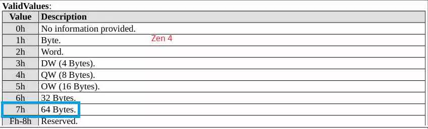
In addition, the implementation of the AVX-512 instructions in Zen 4 assumes that the first level data cache lines and subsequent cache levels have increased the cache line size from 32 to 64 bytes or 512 bits. Which is essential to collect all the data for a single cycle AVX-512 instruction. This small improvement not only means the support for AVX-512 instructions, but the bandwidth of the Load / Store units of the CPU has increased and with it the internal bandwidth of the processor. In addition, the fact that Zen 4 can load 64 bytes of data directly implies that there is a new AVX-512 unit capable of performing these instructions in a single cycle.
The AVX-512 instructions however contain a limitation and it is their high level of consumption. This could cause the Zen 4 CPUs to run below their usual clock speeds when using these types of instructions.
Cache system changes in Zen 4 architecture
| Cache | AMD Zen 4 | AMD Zen 3 |
|---|---|---|
| L1 Data | 32 KB 8-Way | 32 KB 8-Way |
| L1 Instructions | 32 KB 8-Way | 32 KB 8-Way |
| L2 | 1 MB 8-Way | 512 KB 8-Way |
| L3 | 32MB 16-Way | 32MB 16-Way |
| L1 ITLB (MMU) | 64 fully associative inputs | 64 fully associative inputs |
| L1 DTLB (MMU) | 512 inputs 4.Way | 512 inputs 4.Way |
| L2 ITLB (MMU) | 72 fully associative inputs | 64 fully associative inputs |
| L2 DTLB (MMU) | 3072 12-way tickets | 2048 8-way tickets |
Since the first AMD Zen the cache system of AMD CPUs has remained more or less the same. With the exception of the last level cache that is shared by all the cores of the CCD, but in the case of Zen 4 there will be changes in what is the cache structure of the core itself, which you can see in the following table.
The first change to note is in the L2 cache of each core, this will increase the capacity of the 512 KB up to 1 MB memory, which increases the chances of finding the data in said cache, but on the other hand, the L1 and L3 caches remain unchanged in terms of their size. Of course, as we have commented before, the size per cache line has gone from 32 bytes in size to 64 bytes.
There’s also changes to TLB or early translation buffers. They are used by the MMU in each processor core to translate virtual addresses into physical addresses. As you can see from the table that starts this section, the lookahead buffer for top-level data cache has gone from 64 entries to 72 entries. On the other hand, the L2 cache has gone from 2048 entries at 3072 entriess. What supposes an increase of 50% in this aspect and not only in capacity, but also in the number of simultaneous accesses.
RAM memory support via Compute Express Link
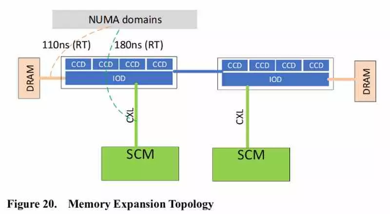
This is where we have to start to differentiate the range of processors for laptops and desktops from the future AMD EPYC under the code name Genoa and that is while the PCI Express 5.0 standard will not be available for CPUs under socket AM5 yes it will be on AMD’s Zen 4-based HEDT and server CPUs and with it the support for CXL.
The key to the CXL standard is that it gives memory consistency to the PCI Express 5.0 interface, which means that the memory modules are either non-volatile memory, RAM, or a combination thereof. they can not only be connected via the classic memory interface, but also through the PCI Express port.
On the market there are already RAM memory expansion modules through PCI Express with CXL, also called Storage Class Memory or SCM. AMD is going to integrate Genoa EPYC into its AMD the ability to expand the system RAM through the PCIe 5.0 interface. Of course, with the counterpart of higher latency in accessing said memory compared to DDR5, LPDDR5 or any other type of memory compatible with which AMD makes compatible CPUs and APUs with Zen 4 architecture.
The use of two different memory wells at the physical level also implies the implementation of DMA mechanisms to copy the data from the two memory spaces, which despite being unified at the addressing level, are not at the physical level, which means that they need a mechanism to copy data from one RAM space to the other.
Greater internal and external bandwidth
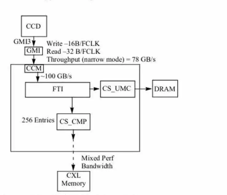
There is a detail that has not been said in all this and that is that AMD uses its Infinity Fabric interface to communicate both internally and externally the different components. IF interfaces with a bandwidth of 32 bytes have been used to communicate caches with each other for several generations of AMD Zen and the jump from 32 Bytes per cache line to 64 Bytes also represents a jump in that aspect and that the amount of data circulating inside the CCD and CCX with Zen 4 architecture has doubled compared to Zen 3.
However regarding communication with the Northbridge or IOD it does not seem that there will be changes and the GM portI communicating the CCD Chiplets that will contain the Zen 4 cores will still have a 16 bytes / cycle for writing and a 32 bytes / cycle for reading bus at the clock speed of the IOD. Which we remember that in Zen architecture depends on the clock speed of the DRAM controller used. In the diagram extrapolating the bandwidths we can deduce that the clock speed of the IOD is 2400 MHz, which corresponds to the memclk of the DDR5-4800.
Nor can we forget about IO Hub. Which is also in the IOD or Northbridge and is responsible for communicating with the peripherals. Being one of the parts that has also received improvements as a result of the support of the new I / O interfaces. As is the case with USB4 and PCI Express 5.0. So AMD has increased su bandwidth from 750 MHz to 1150 MHz.
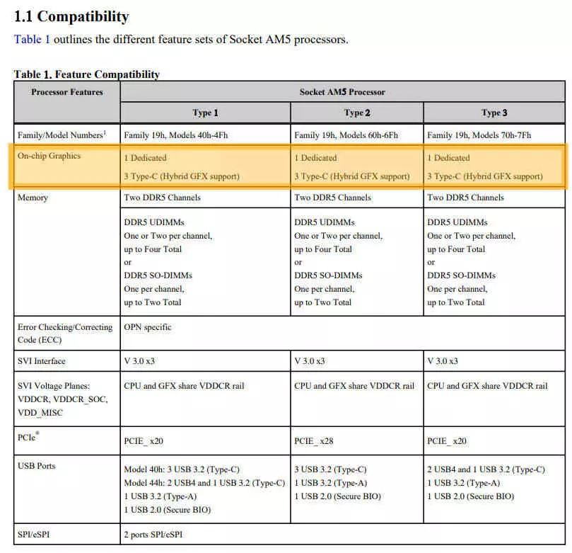
Which serves to the maximum number of PCIe 4.0 lanes has increased from 24 lanes to 28 lanes. This means that motherboard manufacturers can integrate a second M.2 NVMe SSD drive or a USB 4 interface. Of course, these 4 additional lines will not be available in all Zen 4 compatible chipsets as can be seen in the table that accompanies these last two paragraphs.