Integrated circuits, whether they are processors, memories or combinations thereof, are mounted on top of a Printed Circuit Board, which has the appearance of a board where, for those who do not look at hardware and consumer electronics products, it is still a simple support to place the chips. But they are more than that and a fundamental piece in the construction of the hardware components of our computers.
What is a Printed Circuit Board?
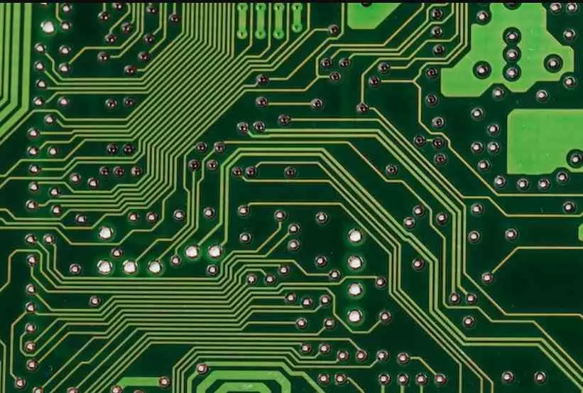
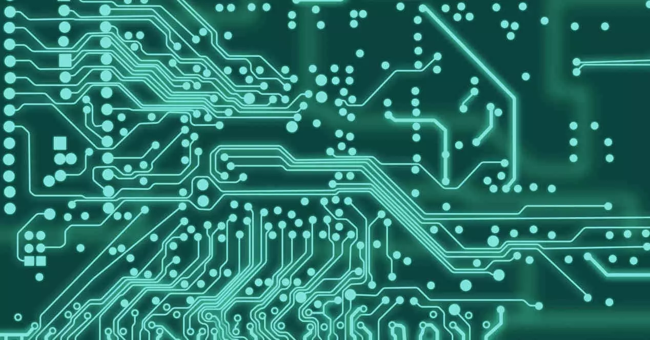
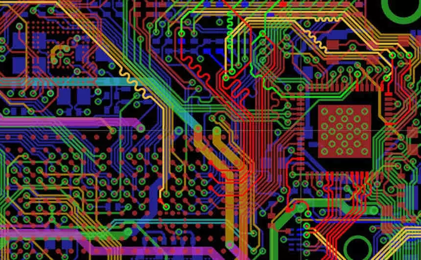
When we look at any motherboard or graphics card we can see how all its components are soldered and well arranged on a surface, which we call Printed Circuit Board or also known by its acronym: PCB. Its usefulness is not only to have the different processing and memory chips placed, but to include the wiring for intercommunication between them, which are the tracks that can be seen on the surface of it.
When prototyping is carried out, what is often done is to use those plates where the pins of each chip are placed in each of the holes and cables are used to interconnect said chip with the substrate. These types of boards are called Breadboards and they are ideal for prototyping systems with the chips already made, but for the final product you will not want a mess of cables, other than that you will want everything to stay in place.
And how does a Printed Circuit Board work? They are really nothing more than a series of copper tracks or other electrically conductive element combined with layers of a non-conductive material. We can have several layers of non-conductive material and in each of them there is a group of copper tracks that are used as wiring to communicate the chips. Although these are not visible and then they are very difficult to read.
How are they made?
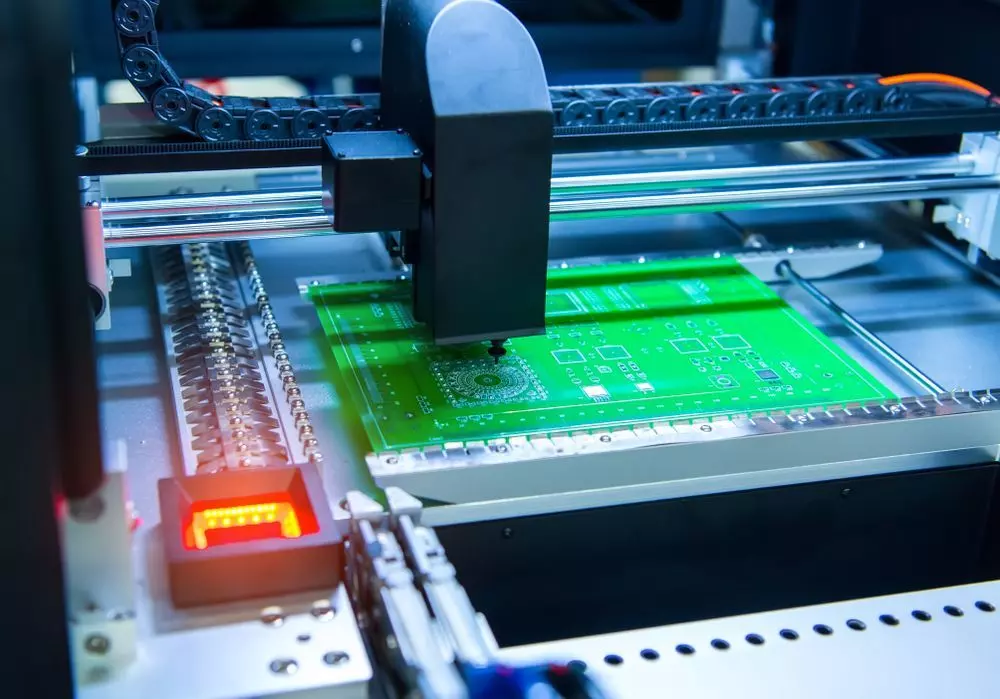
Printed Circuit Boards can be manufactured by a pcb manufacturer in China with a large number of different substances, although the most widely used is a compound called FR-4. Which is composed of a combination of fiberglass and epoxy-type resin, which stands out for its fire-retardant capabilities and is the non-conductive part of the PCB and therefore the one that will not let electricity pass, thus avoiding signal problems.
The Printed Circuit Board also has a complete layer of copper or other conductive material between the two FR-4 layers and use of chemical agents is used to expose the part of the copper that corresponds to the tracks. In order to fit the pins of different chips and electronic components for their placement, holes of a certain diameter are made that will allow the different chips to be connected for a subsequent soldering of each of the pieces. In the case that a socket is used, this will be the one that will be soldered directly to the Printed Circuit Board.
In the case of designs with several layers, each layer has to be much thinner than a model with a single layer and as they increase in number it has to decrease in thickness. Thermal methods are usually used to join them, but they have their problems, since they make the manufacture of base plates more sensitive. This way of working also
How are they designed?
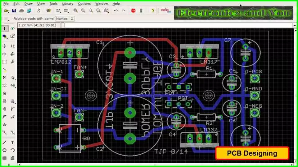
To design them today they are used specialized computer programs that allow us to draw the PCB and even simulate operation of each of its connections to verify that the signal is transmitted properly. Examples of this type of application are the Autodesk Eagle, Circuit Maker, etc. Of course, we are talking about a circuit that combines analog and digital electronics, so designing one requires knowledge of this discipline.
Once it has been seen that the circuit works in the simulation, there are two options:
- On the one hand, you can hire a company specialized in its construction to manufacture a few versions of your design. So you do not need to have the necessary equipment at home to do it and you can use your time on other tasks or for your free time, but you will have to wait to have them ready.
- The other option is to create your own PCB from home, we have a complete tutorial on it in case you are interested and want to know how to do it.
For fans of computer-focused electronics, the design and creation of Printed Circuit Boards is one more part of their creation process, whether it is to create projects from scratch or even to restore an old system in which due to poor condition of the components no longer function properly.
Is it worth creating my own PCBs?
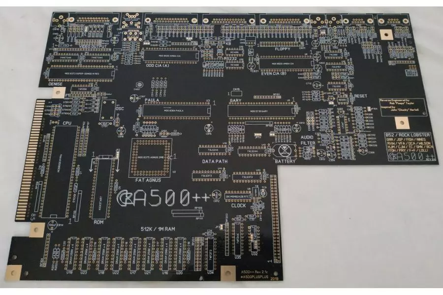
This is a question that some of you will be asking yourself when reading this article and from the perspective of the writer of this I would tell you that it is very worthwhile and it is a very rewarding introspective work and it is essential if you are looking to restore old systems. What’s more, if you create your own solutions composed of a combination of FPGA, CPLD and other components, both at an amateur and professional level, you are going to need your own Printed Circuit Board.
Unfortunately today many contemporary products that make use of multi-track Printed Circuit Board where it is almost impossible to reverse engineer by looking at one of these boards and creating a replica, but when restoring old systems or creating small improvements for themselves it is possible.
Of course, it will not help you to restore very advanced hardware elements such as current graphics cards, since their assembly is carried out by very high precision machinery creating tracks in an extremely complex way and making use of multilayer PCBs.
So in the end it depends on the application that you are going to give your design, but you can always give it a commercial outlet, either with new creations or by bringing old systems back to life. Either way, it is part of the process of creating the new hardware.