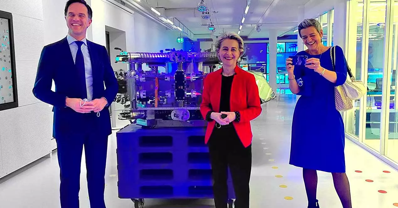
Today was D-day, today the EU has revealed all the main ins and outs of what will be its commitment to the semiconductor sector, aware that whoever dominates it is subjugating the rest of the world. The bet is at the same level as that of the US, precisely at the same level as Thierry Breton advanced, where the objective is clear: to dominate the 2nm in just 8 years and reverse the flight of talent and global share in semiconductors. So is the EU Chip Law by 2030.
Úrsula Von Der Leyen and Thierry Bretón himself have been in charge of giving the details and, as we will see below, the plan is even more strategic than that of the United States and much more than that of China. Will we be able to compete and recover what we lost? Everything points to yes.
EU chip law: 45 billion euros in 8 years
Europe is the world’s center for semiconductor research.
And we are strong in specific sectors, such as chips for cars and for Industry 4.0.
But I want us to become a strong player all across the value chain. And for that, next week we will present the first-ever #EUChipsAct. pic.twitter.com/QskGZCljql
– Ursula von der Leyen (@vonderleyen) February 6, 2022
This is the round figure for the 27 of the EU, where it will have a very clear objective that we already advanced last week: multiply by four the production on national soil of chips with a deadline in 2030.
And it is that according to the current scenario, up to three quarters of the FAB for chips are in Asia, where to be specific, 92% of the most advanced nodes come from Taiwan, from TSMC specifically. IMEC CEO Luc Van den Hove explains the approach that the EU will follow:
“This is a very interconnected ecosystem where we depend on others. It is very important that we make sure that Europe strengthens its position so that we too create reverse dependencies.”
Basically what has been turning the tortilla around. If the law has seen the light today, it is because the EU already has contracts with Intel, TSMC and Samsung to create gigantic FABs, where we also know the main points of the distribution of those 45 billion.
Three tiered grant packages
Thierry Breton explains very clearly how the investment game will play out in this EU Chip Law:
“We will have three main packages: one will be to support R&D with grants of between eleven and twelve billion. The second part is to support the FABs and MEGAFABs, that means thirty billion euros of public money. And the third part will be to support emerging companies or start-ups with a fund of two to five or six billion specifically for it.
The objective is clearly marked: first, the money will be allocated to the FABs and MEGAFABs for their prolonged construction time, where when they are assigned and construction begins, R&D will begin in adjacent or specific centers designated for that purpose, and finally support for emerging companies will be developed in parallel.
With this it is expected that the production lines start with the current 10nm (Intel and TSMC possibly) to advance in a period of 8 years at 2nm and lower as well as heterogeneous 3D SoIC processes to integrate various matrices, as the Taiwanese and also the Blues do. With this, Europe plans to climb from 10% of the world share of semiconductors to twenty% for said 2030.
A plan that is as advanced as it is risky and tough, because what is needed is a company that competes with the big three, a process in which we are immersed with the only FAB of our own that we have in Germany. We will see if Europe finally manages little by little to place itself where it belongs.