Competition in the world of semiconductors is fierce. TSMC is the undisputed leader when it comes to chip manufacturing, since the designs are carried out by its customers, but IBM is not about to be left behind in the nanometer raceand has already defined a strategy to improve its position in this sector, an alliance with the Japanese company Rapidus.
This alliance with the Japanese semiconductor consortium Rapidus will have, as its main objective, to establish a chip production line at 2nm in the first half of 2025. This first production line will work with prototypes, which means that they will not be commercial units, and therefore it is a risk phase that will represent a very important investment for both companies.
If that first move goes well, IBM and Rapidus will put themselves in a prime position within the semiconductor industry, and will be right up there with TSMCsince the Taiwanese company also plans to start producing chips in the 2 nm node by 2025, as long as things go according to their own forecasts, obviously.
Right now we are in an important transition stage. The 5nm node is the most popular today, but the jump to the 3nm node will become a reality very soon, and this year its adoption by some giants of the sector will begin. Except for a last-minute surprise, Apple will be the first to launch a SoC for smartphones based on TSMC’s 3nm node, the Apple A17, which will be used in the iPhone 15 Pro and iPhone 15 Pro Max.
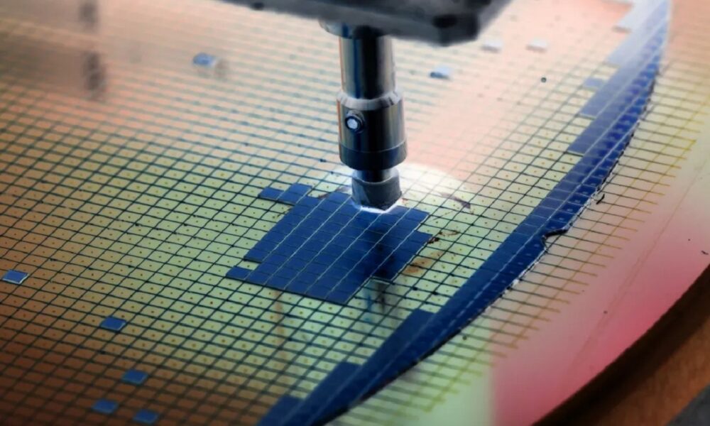
Leaps in the manufacturing process are important because reduce the size of the transistorsand make it possible to introduce performance and efficiency improvements. It is also possible to reduce the space occupied in the silicon wafer, which in the end translates into a greater number of chips per wafer, with all that this entails in terms of manufacturing costs.
However, by reducing the size of the transistors logic gates become thinner, and this increases the risk of electrical leakage. It is also more difficult to achieve a good success rate on the wafer, especially in complex designs, and this translates into fewer functional chips. The jump to 2 nm could be very difficult, since it is a value that brings us closer to the physical limits of silicon, so it will be interesting to see how the industry progresses in this new adventure.