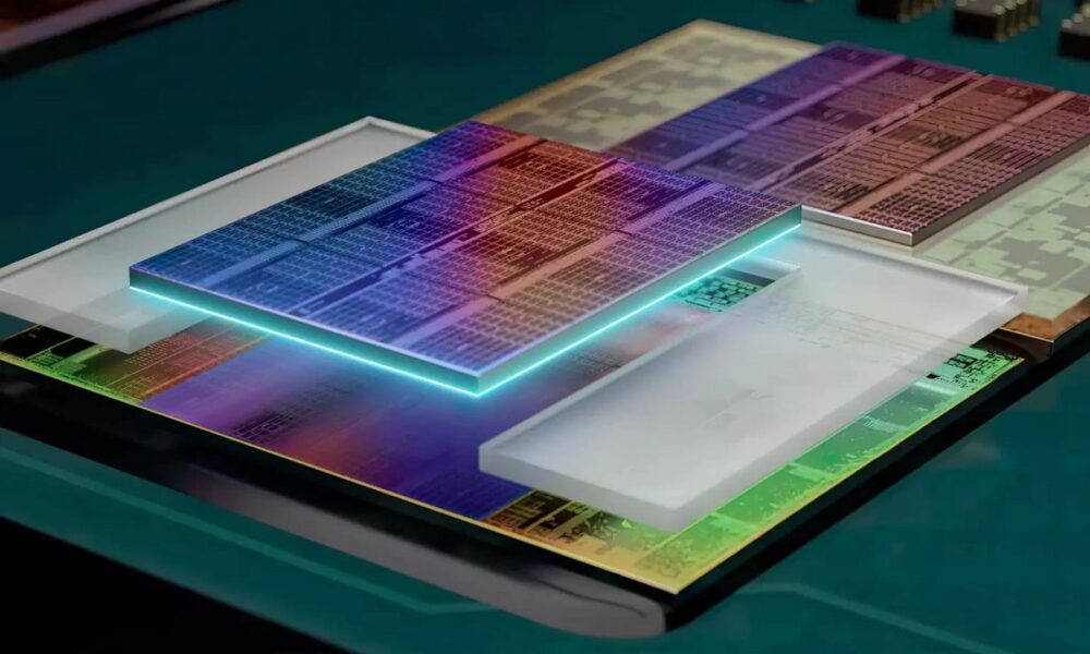
Sources within the industry say that TSMC is preparing a significant price drop that it will affect the 3 nm node, and that this will have as its main objective to compensate for the reduction in orders that the Taiwanese giant is beginning to suffer, and also improve the value and interest around said node.
The drop in demand for semiconductors is not the only problem TSMC has to deal with. This giant’s 3nm node is undoubtedly one of the most advanced nodes in the world, and the machinery required to make chip wafers under that node is overwhelming, so it stands to reason that the cost of each wafer is high. However, there is a detail that plays a very important role, and it is the success rate per wafer.
According to the sources of this information the 3nm node of TSM has a success rate per wafer less than 50%, which means that less than half of the chips that can be made from a wafer are functional. This makes the real cost of accessing this node more expensive, and negatively affects the real value it offers to customers.
It is true, however, that the jump to 3 nm promises an increase in logic density of 60% and an improvement in efficiency of between 30% and 35%, but with a $20,000 cost per wafer and with such a low success rate it is clear that the cost-performance per wafer is far from good.
That’s where that reduction in the price of each wafer comes into play. To attract its largest customers (AMD, NVIDIA, Apple, MediaTek and Qualcomm, among others), TSMC will lower the cost of 3nm wafers, a move that coupled with the gradual maturation of the 3 nm nodeand the corresponding increase in the success rate per problem, will end up being key to accelerating the jump to said node.
The Taiwanese company has no choice, since in the end the 5nm node is still an option for many large that they might even consider reusing that node in their future products. AMD, for example, used the 7nm node on several occasions, and NVIDIA had no qualms about using the 12nm and 8nm nodes.


