Intel has always been the third in contention when it comes to GPUs, after all it is not their main business and it is about something more than what they do that are CPUs. Although in recent years they have increased resources and have a series of gaming GPUs on the starting ramp. However, its architecture has a series of differentiating points with respect to its competition.
The Execution Unit, the foundation of Intel GPUs
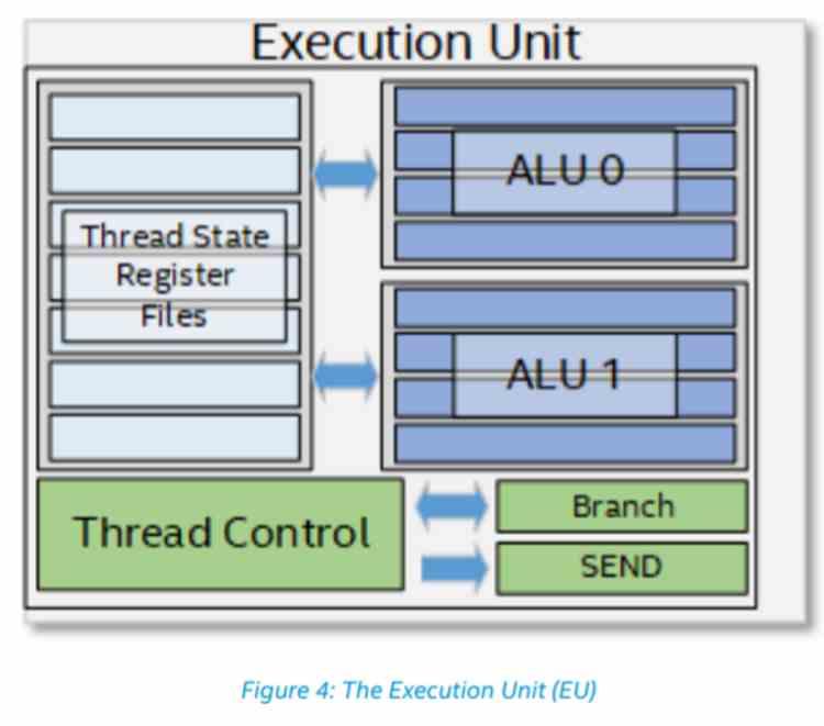
To understand the difference in the organization or architecture of Intel GPUs compared to the rest, we have to understand that while in an NVIDIA or AMD GPU the shader unit is the minimum unit, in the case of Intel’s it is the Execution Unit. what exactly does it consist of? Each Execution Unit is a processor designed for parallelism at the level of the execution thread or full TLP. Therefore, it has a control unit, the records and the corresponding execution units. Which are two SIMD units of 4 32-bit floating point ALUs and another 4 of integers, which are switched and support SIMD over register.
Thanks to the SIMD on register, by subdividing the ALUs and their associated registers, they can work with twice the number of operands per clock cycle for each subdivision made in precision. Thus, they can perform twice as many 16-bit floating-point operations as 32-bit, but four times more if they are 8-bit. As for the functionality of the Execution Units, they are in charge of executing the Shader programs, after all they are the equivalent of the SIMD units of the Intel and AMD GPUs and therefore their task is the same.

In the Intel Xe, the Raja Koduri team has made an important change in the control unit, since now two Execution Units share the same control unit. A change that is very reminiscent of the one that AMD has made in its RDNA architectures where two Compute Units are grouped into a single Workgroup. Something that should not surprise us by the brain drain from AMD to Intel. This change has meant that the control unit has been updated, which surely represents a complete change in the internal ISA of Intel GPUs for a much more efficient one.
Sub-Slice, the Shader unit

The equivalent of shader units that NVIDIA and AMD GPUs have, we have already seen that it is not the Execution Units, but rather the Sub-Slices. Within them you will find the Execution Units grouped. Because each Execution Unit is a subset of a subslice and the Slice is the superset of the subslice, we will see the latter later. Each subslice houses 16 Execution Units inside, which translates into 64 FP32 ALUs and 64 integer ALUs in total. A figure that makes these units equivalent in gross computing power to their AMD equivalents, Compute Units.
As for the rest of the elements that we can find inside the sublice, they are the classics of a unit of this type, although Intel uses different nomenclature than usual. How is the case of the so-called 3D Sampler, which is still the classic unit for handling and filtering of textures, simply Intel has given another name to this classic unit of fixed function that is found in all 3D graphics processors since its inception.

However, the Media Sampler is a much more interesting piece as it is unique to Intel GPUs, it is composed of a series of fixed function units, which are the following:
- The Video Motion Engine provides pixel motion estimation, which is key for video encoders.
- The Adaptive Video Scalar is a unit that executes image smoothing filters.
- De-Noise / De-Interlace is a unit in charge of reducing noise in an image on the one hand and on the other for transforming video in interlaced mode into progressive mode.
Starting with the Intel Xe, the Media Sampler has been withdrawn from within the subslice and has become a fully independent unit. Which continues to be a differential piece with respect to the designs of NVIDIA and AMD.
The Slice, another common piece in GPUs
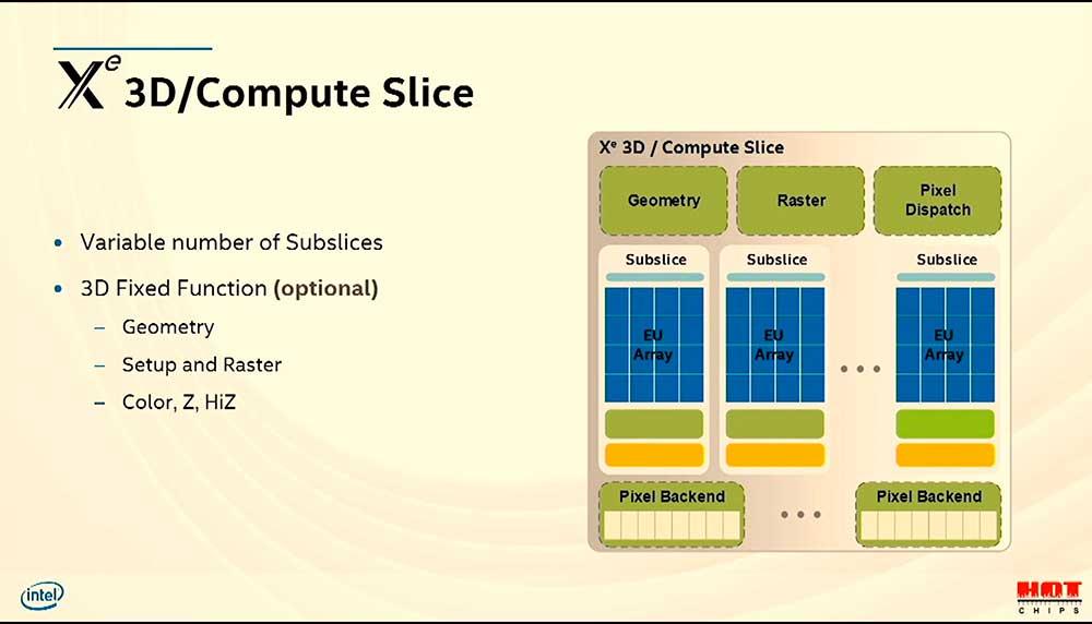
The Slice in the Intel GPU architecture is the equivalent of the Shader Engine or the GPC in the case of NVIDIA. Different names for an organization of units from each other. Inside are the subslices and a series of fixed function units, which are common with the GPUs of other companies.
Although again the nomenclature can be confusing, for example in the rest of architectures the raster unit is usually unified and the unit that generates the depth buffer, both elements occur in the raster phase in a common unit in the case of NVIDIA and AMD, but Intel does it separately.
The same goes for the Pixel Dispatch and the Pixel Back-End. Functions of the ROP units that are performed here by two different elements. After all, the task to be carried out in both cases is the same.
The Intel GPU cache hierarchy

One of the differentiating points of the common architecture of Intel GPUs, compared to AMD and NVIDIA, is precisely how the cache hierarchy is organized. In the case of AMD we find that the RX 6000 have a hierarchy of four levels if we count the newly incorporated Infinity Cache. In the case of NVIDIA, the cache hierarchy is different from that of Intel and AMD, but it is not about the competition to Intel that we want to focus on this article as it is not dedicated to them
The diagram in this section indicates the internal communication within the GPU, both at the subslice and slice level. In the case of subslice we have the classic data cache and shared local memory. But unlike NVIDIA and AMD GPUs, Intel has traditionally added an additional L2 cache that can be accessed by both the 3D Sampler and Media Sampler. Which makes the GPU’s L3 cache the top-level GPU cache.

The differentiation between the L1 cache for data and therefore for the Execution Units and the L2 for the textures has changed in the Intel Xe, where both have been combined into a single L1 cache of data and textures. So now they have a totally standard configuration compared to competitive GPUs.
Another change is in terms of the L3 or last level cache. Contemporary GPUs support the so-called Tiled Caching, which consists in that they rasterize by tiles, but they do it on the last level cache and there is a danger that the data will fall into memory where the energy cost of recovering it skyrockets, so They have increased it from 3 MB to 16 MB.