The word chiplet a few years ago sounded ridiculous to us, but today it has become a secure future. Especially due to the fact that it brings with it a reduction in costs and breaks with the limitations of the monolithic system in terms of cost and size. So it is completely normal that the industry will end up developing a universal connector between chiplets that they have baptized as UCIe.
With the increase in the production costs of processors, the adoption of chiplets to build with several chips what was previously done with just one is a reality. At the PC level, each and every one of the great hardware designers has already launched or has just around the corner an architecture built in this way. So sooner or later they had to agree on the creation of a universal connector that would allow the chiplets of the different brands to communicate with each other.
Industry Launches Universal Chiplet Interconnect Express
The three largest foundries in the world (TSMC, Intel and Samsung) together with a series of technological partners such as ARM, Google, Meta, Microsoft and Qualcomm have launched a new standard. Which consists of a communication interface that they have baptized as UCIe or Universal Chiplet Interconnect Express. Which serves to intercommunicate the different chiplets mounted on a common substrate. That is to say, a processor that instead of being made up of a single piece is made up of several that are interconnected with each other.
The new UCIe standard sIt is based on PCI Express with Compute Express Link and among other things, it will allow the creation of chiplets made up of parts from a single manufacturer, if not that we will be able to see architectures where not only elements with different manufacturing processes are combined, but also from different suppliers. Which completely changes the current paradigm, since until now solutions of this type tend to focus on solutions from the same manufacturer as there is no universal standard to date.
In any case, the existence of the new standard is not something that should surprise us, especially given the fact that collaborations between foundries for the creation of different parts of the same CPU, GPU or APU will be increasingly common. We have the perfect example of this in the collaborations between Intel and TSMC for future projects of the first.
What are the characteristics of the ICU?
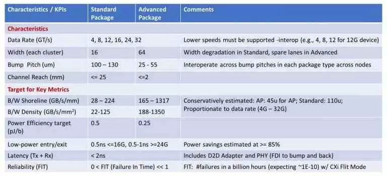
At the moment the standard is not final, but they have released a series of initial specifications in the form of version 1.0 of the standard. Which comes with two different types of interconnections. Let’s not forget that these refer to vertical interconnections of each of the chiplets with respect to the interposer, which is the communication substrate on which they are mounted to transmit the signal and, therefore, the data. This allows them to reach bandwidths above one terabyte per second at consumption levels up to 0.25 pJ per transmitted bit.
Translated into something that can be understood in conventional language, it must be taken into account that the transfer speed to traditional RAM is currently usually between 6 and 8 pJ/bit on average, depending on the type of memory used. Low consumption is one of the keys to this type of interconnections, which are designed to transmit large amounts of bandwidth between the different components. Which is key for CPUs made up of dozens of cores in the server market, as well as GPUs made up of chiplets.