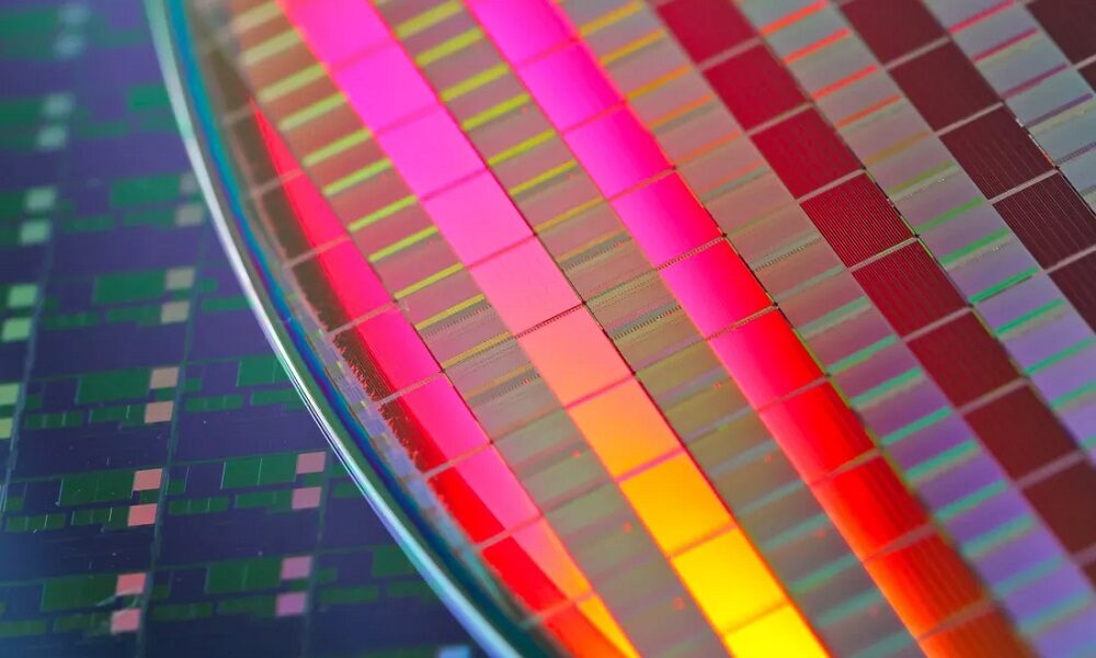
Leaps in manufacturing processes are very important because, as many of our readers will already know, they allow reduce the size of the transistors and increase the density thereof. They also allow the introduction of design optimizations that ultimately translate into performance and efficiency improvements. CPUs and GPUs are two of the types of chips that benefit most from leaps to new manufacturing processes, but this reality is starting to change.
According to TSMC, the world’s largest semiconductor manufacturer, the transistors in SRAM memory used in CPU and GPU caches is stopping scaling with each node hop, that is, you are not reducing the size of your transistors, and this is a problem for many reasons. The first is in the space occupied at the silicon level, and that is that a cache with the same size of transistors in CPUs and GPUs that have smaller and smaller transistors takes up a huge amount of space compared to the rest of the elements.
On the other hand, we also have two major problems, the same benefits are not achieved when jumping to a more advanced node, and production costs increase because the impact on the wafer is still high, due to that size issue that we have already mentioned (its transistors are still just as big even if a more advanced and expensive node is used, and they occupy the same space on the silicon wafer).
For the big players in the sector, this could become a major obstacle that not only will make future designs more expensive, Since in the end both CPUs and GPUs use caches of different levels, it will also prevent certain architectures from reaching its maximum peak of miniaturizationsince the cache will still be “huge” in comparison.
TSMC has already confirmed that SRAM memory made with the 3nm node will have the same density of transistors than SRAM memory manufactured in the 5 nm node, which is precisely the one used in AMD’s Ryzen 7000 processors. The upgraded 3nm node, known as the N3B, doesn’t paint a much better picture either, as it will only be able to reduce the size of SRAM’s transistors by 5%.
In the attached graph we can see the scaling of the different TSMC nodes applied to the SRAM, and it makes two things clear, that the jump from the 7nm to the 5nm node represented a very small improvement in the reduction of the occupied area, and also that stagnation that we will suffer with the jump to 3nm. If we continue the current trend, SRAM will have an increasing density of transistors, but these will not shrink fast enough, and they will take up more and more space.
AMD has already taken action on the matter in this regard, and it is no coincidence that heThe infinite cache of its Radeon RX 7900 XT and XTX graphics cards has been externalized to 6 chiplets. This has avoided having to embed them into the GPU, something that would have resulted in a huge chip.


