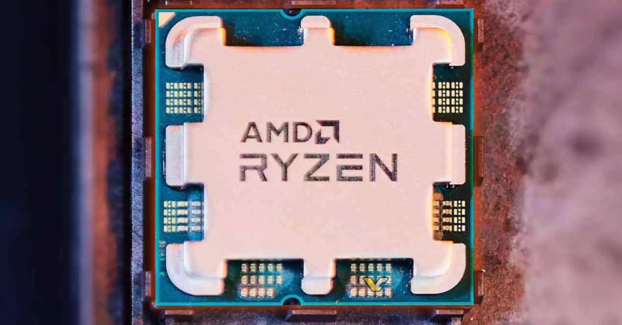
Therefore, we are already clear that PCI-Express is nothing more than an interconnection interface; is developed by the PCI-SIGwhose existence we could broadly define as a consortium of manufacturers and designers who agree to create an interface with certain requirements, so that their devices can work in tandem and, precisely, communicate with each other following these requirements.
This interface has been developed since 2003 to the present day, and began as an evolution of the AGP and PCI standards. The PCIe 1.0 version, introduced in 2003, was quite simple but already represented great improvements over AGP and PCI, since it had a data transfer capacity of 2.5 GT/s (GigaTransfers per second) and 250 MB/ s for each data path.
If we compare this with the current PCIe 5.0, capable of handling 32 GT/s and 3,938 MB/s via data path, things have certainly changed a lot. But wait, now PCI-Express 6.0 arrives to improve the present again.
PCI-Express 6.0: technical specifications
| Data speed | 64 GT/s (double that of PCIe 5.0) |
|---|---|
| Format | PAM-4 with flow control unit (FLIT) encoding |
| channel reach | SNR provision reduced by 9 dB |
| backward compatibility | Yeah |
| bit error rate | 0.000001 |
| Duplex | Complete |
As usual every time a new generation of the PCI-Express interface comes out, 6.0 literally offers twice the bandwidth of PCIe 5.0, ie 32 GT/s. You are probably aware that when we talk about PCIe sockets on PC motherboards, we do so with a multiplier, such as PCIe 5.0 x16, which is currently used by graphics cards. This is so because, so that we understand each other, they have several “lanes” that work in parallel, so the bandwidth can be multiplied.
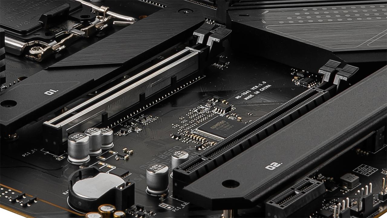
Thus, we can find PCIe interfaces of 1, 4, 8 and 16 lanes sending data in parallel, and with PCIe 6.0 this results in a data flow of up to 256 GB/s (although in M.2 format SSDs this is 64 GB/s maximum). Be careful, because we are talking about the added bandwidth in both directions, that is, reading and writing simultaneously.
backward compatibility
The PCI Express interface has always been backwards compatible with previous versions of the protocol, which means you can plug a PCI Express 1.0 card into a PCI Express 6.0 slot and it will work. This is called backward compatibilityand it is thanks to the fact that the layout of the pins has always been the same in all versions of the interface.

Be careful, because this is also a double-edged sword, since to increase the bandwidth you cannot place additional pins and, therefore, you have to increase the clock speed at which the interface works. In other words, the data pumps per second to transmit the data are faster to generate a greater flow, something that can have drawbacks such as higher consumption and greater heat generation.
The problem with PCI Express 6.0? As we increase the clock speed of an interface, it becomes increasingly unstable, and after six generations they have had to make some changes due to the high speed at which the interface works traditionally. The problem is that to transmit 256 GB/s on a Full Duplex interface, which allows transmitting 1 bit for each direction simultaneously, we need the interface speed to go up to 128 GHz and at those speeds the integrity of the signal is seriously compromised. engaged.
This has forced a series of measures to be adopted to make the jump to PCI Express 6.0 possible, starting with the coding, which is the next thing that we are going to explain.
PAM4 encoding in PCIe 6.0
How does an external or internal interface of a chip know if the value is a 1 or a 0 (remember that we are in binary system)? Actually it is simple: depending on the voltage at which the information is transmitted. Binary systems are based on the use of two voltages with enough distance between them so that the drop or rise in voltage causes the receiver of the signal not to be confused.

What does this have to do with PCI Express 6.0? Since we cannot increase the bandwidth because the signal is distorted, and neither the number of pins because then we would not have backward compatibility, an alternative solution must be found. In the end, they have found it using the encoding called PAM4 (Pulse Amplitude Modulation 4), which we have already seen in GDDR6X memories.
This type of encoding is not based on two values like the binary system, but on a total of four different possible voltage values for each of the pins. In this way, we can encode the values 00, 01, 10 and 11 on each pin: four values in total, instead of the two classic values that would be 0 or 1.
This solution avoids having to increase the bandwidth and the pins, but it tells us that in PCI Express 7.0 it will no longer be possible from conventional methods. We may see the use of photonics and optical interfaces, but with PCI Express 6.0 improvements hot out of the oven, better bear with its successor.
PCI-Express 6.0 no longer communicates… just the same
The jump to PAM4 has also changed the way in which the PCI Express 6.0 interface sends its packets, despite the fact that it is compatible with previous generations, which make use of the previous system called PAM2 or NRZ. The reality is that the PAM4 format does not support the older packet system and therefore the communication protocol has changed because of it.

We have mentioned before that the high speed of PCI-Express 6.0 can cause instability, and with it come errors, which is why it has also been necessary to integrate a new error correction protocol called Forward Error Correction, or simply FEC, and that you can see represented in the diagram above. The downside is that this has added another problem, which is that latency has been significantly increased by having to pass each data packet through the error correction system.
To alleviate this, the PCI Express 6.0 standard uses a type of packet called FLIT. A packet is nothing more than a set of bits with a specific destination. The sending latency of each FLIT? Depends on the number of lanes in the interface, but each packet has a latency of only 2ns on a 16-lane PCI Express 6.0, but up to 32ns on a single-lane interface.
The FEC only works with fixed sizes, and that is why the FLIT has a size of 256 bytes per transmission. Each packet or TLP can have a size ranging from 0 bytes to 4096 bytes and, therefore, each packet can be made up of several FLITS.

And this is where the cyclic redundancy check comes in, known as CRC in English for its acronym «Cyclic Redundancy Check». It is a code error correction system that is commonly used in storage units and digital networks, and that has been integrated into the PCI-Express 6.0 standard to verify that the data transmitted from end to end maintains its integrity. and not a single bit has been changed in the process.
This is achieved with a series of polynomial calculations carried out by a series of specialized units that are included with the interface. This makes sense with the huge amount of data to be transmitted and is a savings especially for future SSD manufacturers who will not need to add this functionality to their drives as it comes standard on the interface itself.
Low Power Mode in PCI-Express 6.0
Finally, it is interesting to note that PCI-Express 6.0 adds a new state of low consumption baptized as L0P. This mode allows the interface to cut its power consumption when the data rate being sent is below its maximum. To do this, it is capable of modifying the clock speed at which the connected device needs for specific moments in which the data to be transmitted is less in volume.
This mechanism is closely related to the new technologies introduced in the sixth version of PCIe 6, so it can only be used with devices compatible with this generation of the interface (in other words, for LoP low-power mode there is no backward compatibility, it will only work with devices that have native PCIe 6.0 support).