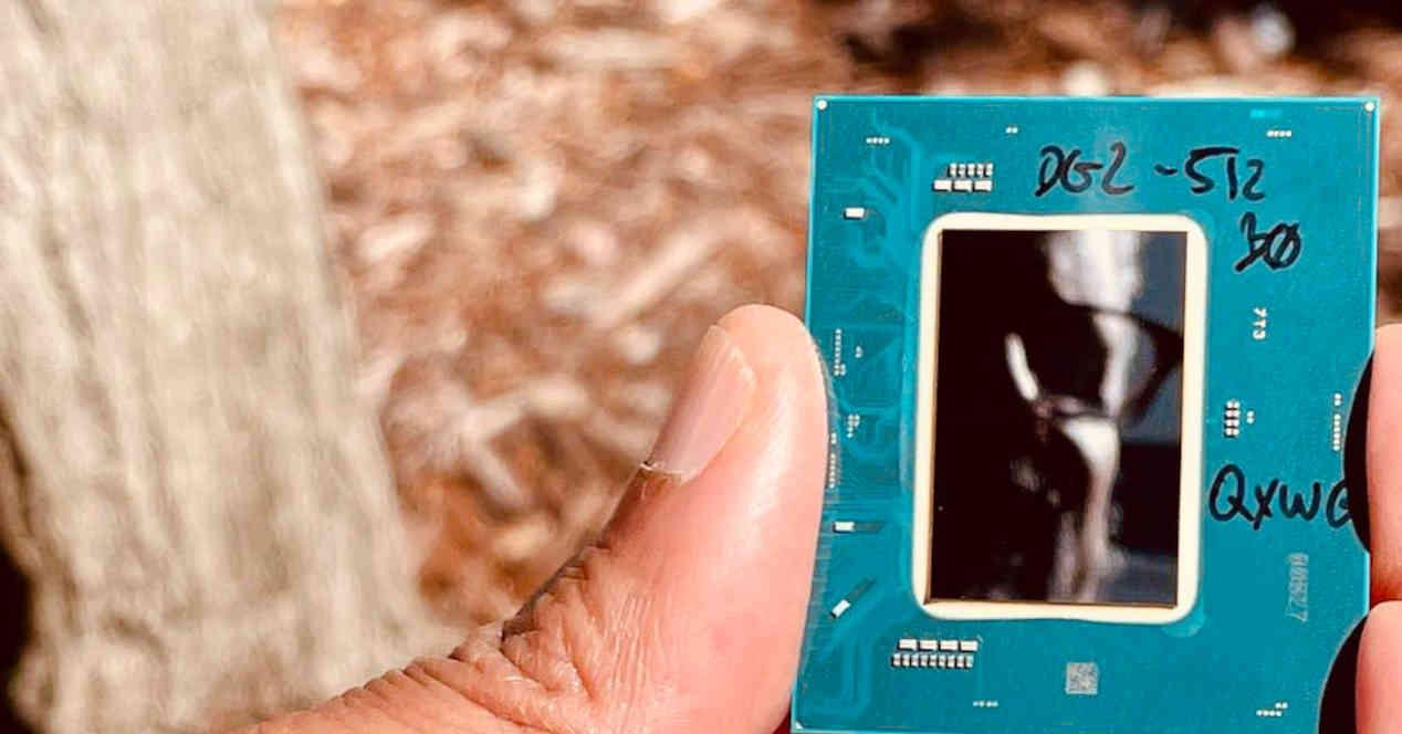
In the case of Zen 3 it meant that the AMD tortoise outperformed the free Intel. However, the appearance of the Alder Lake architecture of the Intel Core 12 has once again given the crown to the blue mark as the winner of the moment. And with the Raptor Lake architecture and the Intel Core 13 just around the corner, AMD has no choice but to react with Ryzen 7000, based on a new architecture: Zen 4.
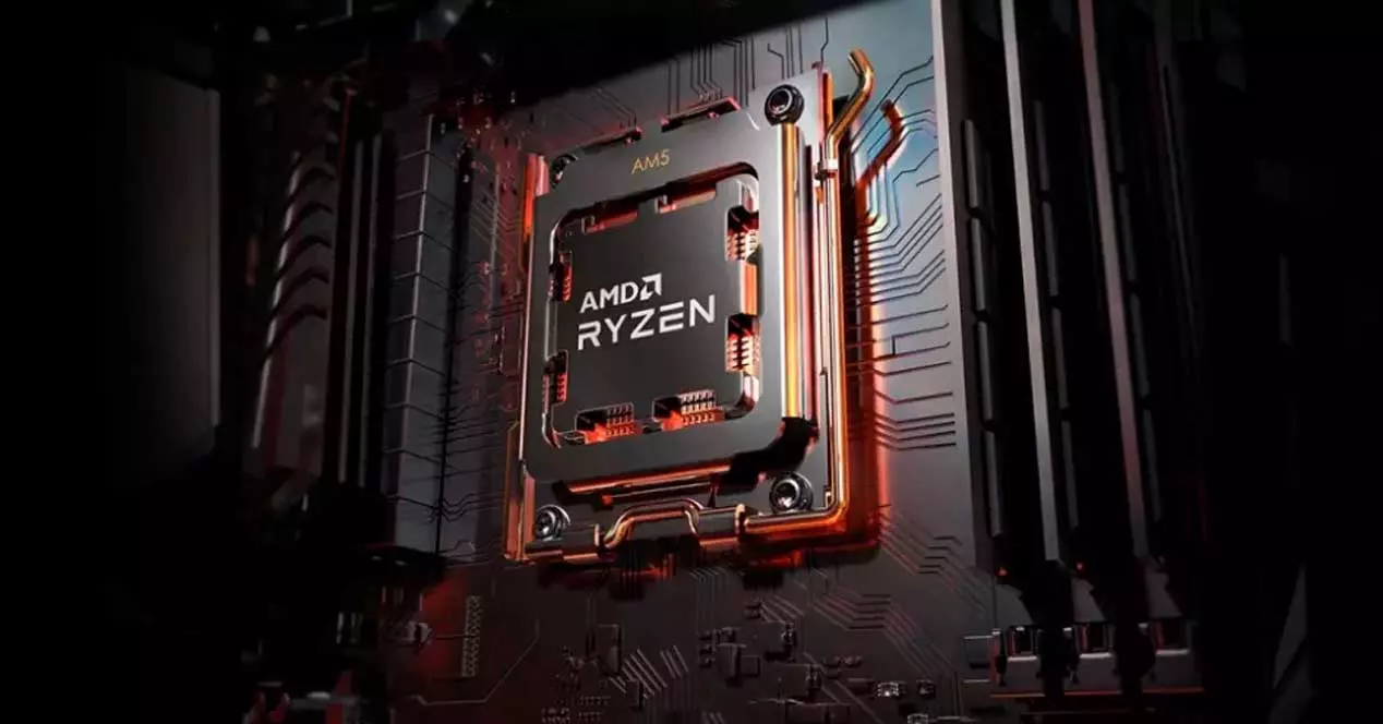
Core configuration in the Ryzen 7000
The Zen architecture encompasses the cores in something that AMD calls CCX, which consists of a series of cores with the following characteristics:
- Each core has the first and second level cache private, that is, the rest of the cores cannot access it.
- The L3 cache is shared and has access to all of them. In addition, the different cores communicate internally through a network of Infinity Fabric interfaces.
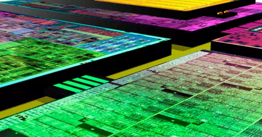
- In Zen and Zen 2 each CCX was made up of 4 cores and their shared L3. In Zen 3 it went from 4 to 8 cores. Zen 4 will have the same type of configuration as Zen 3 and therefore 8 cores per CCX.
As far as power is concerned, this time AMD has made a double improvement for performance. First of all, it has increased Boost speeds of over 5GHz for all processors, which combined with the 15% performance per clock cycle gives an average of 40% more power than Zen 3 compared model. with model. However, this has meant that the TDP has increased from 105 W to 170 W.
Zen 4 architecture will integrate AVX-512 instructions
The first important novelty will be in the support for AVX-512 instructions, which until now had been exclusive to Intel CPUs. These instructions, as their name suggests, are 512-bit long SIMD instructions, the longest ever used on an x86 architecture CPU. However, AMD will only support a subset geared towards speeding up AI algorithms. Unofficially, it is known that AMD will support the following extensions in the Ryzen 7000 Zen 4 cores:
- AVX512VL
- AVX512BW
- AVX512CD
- AVX512_IFMA
- AVX512DQ
- AVX512F
- AVX512_VPOPCNTDQ
- AVX512_BITALG
- AVX512_VNNI
- AVX512_VBMI2
- AVX512_VBMI
- AVX512_BF16
Also, the implementation of the AVX-512 instructions in Zen 4 means that the first level data cache lines and subsequent cache levels have increased the cache line size from 32 to 64 bytes or 512 bits. Which is essential to grab all the data for a single cycle AVX-512 instruction. This small improvement not only means support for AVX-512 instructions, but the bandwidth of the CPU’s Load/Store units has increased and with it the internal bandwidth of the processor. Also, that the fact that Zen 4 can load 64 bytes of data directly means that there is a new AVX-512 unit capable of performing these instructions in a single cycle.
AVX-512 instructions, however, contain a limitation and that is their high level of consumption. This could cause Zen 4 CPUs to run below their usual clock speeds when making use of these types of instructions.
Changes in the cache system in the Zen 4 architecture
| Cache | AMD Zen 4 | AMD Zen 3 |
|---|---|---|
| L1 Data | 32KB 8-Way | 32KB 8-Way |
| L1 Instructions | 32KB 8-Way | 32KB 8-Way |
| L2 | 1MB 8-Way | 512KB 8-Way |
| L3 | 32MB 16-Way | 32MB 16-Way |
| L1 ITLB (MMU) | 64 fully associative inputs | 64 fully associative inputs |
| L1 DTLB (MMU) | 512 entries 4.Way | 512 entries 4.Way |
| L2 ITLB (MMU) | 72 fully associative inputs | 64 fully associative inputs |
| L2 DTLB (MMU) | 3072 entries 12-way | 2048 8-way entries |
Since the first AMD Zen, the cache system of AMD CPUs has remained more or less the same. With the exception of the last level cache that is shared by all the cores of the CCD, but in the case of Zen 4 there will be changes in the cache structure of the core itself, which you can see in the following table.
The first change to note is in the L2 cache of each corethis will increase the capacity of the 512 KB up to 1 MB of memory, which increases the chances of finding the data in that cache, but instead the L1 and L3 caches remain unchanged in size. That is if, as we have commented before, the size per cache line has gone from 32 bytes in size to 64 bytes.
There’s also changes to TLB or translation-ahead buffers. They are used by the MMU in each processor core to translate virtual addresses to physical addresses. As you can see in the table that starts this section, the translation lookahead buffer of the first level data cache has gone from 64 entries to 72 entries. The L2 cache, on the other hand, has gone from the 2048 entries to the 3072 entriesyes Which represents a 50% increase in that aspect and not only in capacity, but also in the number of simultaneous accesses.
The interfaces for peripherals in the AMD Ryzen 7000
Not all peripheral interfaces are managed by the motherboard chipset, but some of them are managed through the processor, as the so-called IOD chip within the multi-piece composite that is the Ryzen 7000 has three functions.
- Intercommunicate the different CCD Chiplets with each other.
- Manage communication with the memory of the different devices connected internally or externally to the IOD itself.
- Provide connectivity for a number of I/O interfaces found within the IOD, as well as communicate with the motherboard chipset. The subunit in charge of this task is called the IO Hub and it will be on this part that we will focus.
Well, if we talk about PCI Express 5.0, in total we have a 32-line interface inside the processor. Of which, 28 have external connectivity distributed as follows:
- 16 PCI Express 5.0 lanes are for connecting a graphics card. In some models this can be divided into 2 connectors with 8 lines each.
- The remaining 8 lines are divided into two four-way channels. As a minimum and by AMD requirement, one of them must be used for an NVMe PCIe Gen 5 SSD drive.
- 4 lines that connect to the motherboard chipset directly.
- 4 internal lines, which is where the USB interfaces are connected
Interfaces for high-speed USB peripherals on Ryzen 7000
Although not officially confirmed by AMD, we know from other sources that the USB hub inside the IOD on the Ryzen 7000 is connected to a 4-lane PCI Express 5.0 interface. This means that the bandwidth it can take is 128 Gbps or 16 GB/s of bandwidth in total. This figure will be important to understand the configuration.

If we look at the known specifications we will see how AMD announces that the Ryzen 7000 can have up to 4 video outputs for the integrated GPU. However, this is tricky and to understand it we have to see how the connections are divided:
- An eDP connection for an LCD or OLED monitor. Is it possible that we will see a version for laptops of the Ryzen 7000? Who knows, but this could very well be a clue to it. In any case, many motherboards will come with a DisplayPort to HDMI or Standard DisplayPort converter to give the integrated GPU a video output.
- A USB 3.2 Type A 10 Gbps connection. This grants the ability to recover the system BIOS from a USB Pendrive connected to said port. If it is not used for that task, it is a conventional data interface.
And what about the rest of the interfaces Simply with each of them, the creators of the motherboards can choose any of these three scenarios:?
- Add a USB 3.2 port at 20 Gbps, either Type A or Type C.
- Add two ports: a USB 3.2 at 10 Gbps Type or Type C and a low-speed DisplayPort output.
- One video output at 20 Gbps, with full Display Port 2.0 or HDMI 2.1 support. The latter through a converter.
So we can have up to 4 USB 3.2 ports at 20 Gbps each. Which will occupy 80 Gbps of the 128 Gbps allocated for the USB controller.
Where do the 14 USB ports in the specs come from?
One of the enigmas that has made us scratch our heads in the presentation of the Ryzen 7000 at Computex is the statement of “Up to 14 USB ports” in which AMD has not made it clear to us where they come from, whether from the chipsets or from the processor .
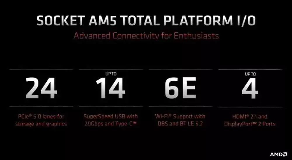
Well, after collecting the pertinent information we have concluded that the controller of these interfaces is located in the processor. How could we have known? Easy, of the 128 Gbps provided by the 4 additional PCIe lines, we already have 80 Gbps occupied, but we have 48 Gbps left. Well, USB 2.0 ports consume 4.8 Gbps of bandwidth, so 10 of them take up that 48 Gbps we have left. With this we have already solved the enigma. Which is not to say that the X670 chipset doesn’t provide additional ports of this nature.
Of the 14 ports, two of them have specific functions within the system:
- One of them has a direct interface with the TPM 2.0 chip to be able to install Windows 11.
- The second for special functions serves as a hub for the SPI/eSPI, GPIO and HD Audio interfaces.
With this we already have the 14 USB ports that will integrate the motherboards for AMD Ryzen 7000 processors. However, we still have PCI Express left.
The new AMD chipset for the AM5 platform?
Once we have described the processor interfaces, we have to talk about the ones that the motherboard chipset incorporates. For AMD 600 series motherboards we have two different versions. On the one hand, the B650 composed of a single chip and on the other the X670 platform where we have two chips chained together. In that case, only one of them connects to the CPU through its 4 associated PCI Express 5.0 lines. While the second is subordinate to the first through a PCIe Gen 4 x4 interface that connects both. Both, by the way, are twins and are called Promontory 21, shortened to PRO21.
The interfaces on each of the chips are:
- 12 PCI Express 4.0 interfaces, 4 of which are used to interconnect both chips in the X670 and X670E with each other. So the B650 has 8 interfaces of this type. Depending on the model
- 4 PCI Express 3.0 Interfaces, each of which can act as well as SATA III at 6 Gbps. In some cases, these connections can be used to integrate high-speed Ethernet connections.
- 6 USB 3.2 interfaces at 10 Gbps per chip. The first two can be in the form of a 20 Gbps port. This is in the case of the B650. If we talk about the X670 and the X670E, then the number of ports of this type that we can connect is doubled.