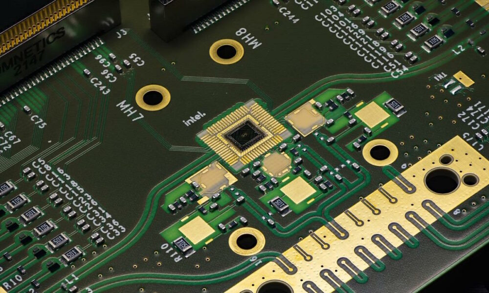
Today, Intel is one of the companies that is betting the most on quantum computing, and it is completely understandable, since this computing model could represent a leap as enormous as the one we experienced, a few decades ago, when we went from vacuum tubes and relays to the age of silicon and transistors. The development of Intel Tunnel Falls It has been the last great achievement of the company in this sector, and as we will see below, it marks an important turning point.
Intel Tunnel Falls is a silicon chip with a power of 12 qubits that the Santa Clara giant has already made available to the quantum research community. We can also confirm that Intel is actively collaborating with the University of Maryland Laboratory for Physical Sciences (LPS) and College Park’s Qubit Collaboratory (LQC) to further advance the world of quantum computing.
And why is Intel Tunnel Falls so important? Well, it’s very simple, because it’s the chip giant’s response to the needs of the main academic institutions and research centers dedicated to quantum computing. They don’t have high-volume manufacturing equipment like Intel, and that new 12-qubit chip allows researchers to immediately start working on their projects instead of trying to make their own devices.
This opens up a whole new world of possibilities and accelerates research in the world of quantum computingmaking possible a wider range of experiments that allow us to learn more about the fundamentals of qubits and quantum dots, as well as develop new techniques for working with multi-qubit devices.
Jim Clarke, director of Quantum Hardware at Intel, commented:
Tunnel Falls is Intel’s most advanced silicon spin qubit chip to date and takes advantage of the company’s decades of experience in designing and manufacturing these types of transistors. The launch of the new chip is the next step in Intel’s strategy to build a complete commercial quantum computing system. Although there are still fundamental questions and challenges to be resolved on the road to a fault-tolerant quantum computer, the academic community can now explore this technology and accelerate research development.”
Intel is also collaborating with LQC as part of the Qubits for Computing Foundry (QCF) program through the US Army Office of Research, and this is key to supplying Intel’s new quantum chip to research labs. Collaboration with LQC will help democratize Silicon Spin Qubits, This will allow researchers to gain practical experience working with scale arrays of these qubits. This initiative aims to bolster workforce development, open the doors to new quantum research, and grow the overall ecosystem.
Going deeper into the design of Intel Tunnel Falls we are, as we have already said, facing the first Intel silicon spin qubit device that is made available to the research community. Has been manufactured in wafers of 300 millimeters at Intel’s own D1 manufacturing facility, it is 12-qubit powered and takes advantage of Intel’s most advanced industrial transistor manufacturing capabilities, such as extreme ultraviolet (EUV) lithography and gate and gate processing techniques. contacts.
As some of our readers will know, in silicon spin qubits the information (the 0/1) is encoded in the spin (up/down) of a single electron. Each qubit device is essentially a single electron transistorallowing Intel to manufacture it using a flow similar to that used in a standard complementary metal oxide semiconductor (CMOS) logic process pipeline.
Intel believes silicon spin qubits are superior to other qubit technologies for the synergy it offers with state-of-the-art transistors. Being the size of a transistor, they are up to a million times smaller than other types of qubits that measure about 50 square nanometers, allowing for much more efficient scaling. On the other hand, the use of advanced CMOS manufacturing lines allows Intel to use innovative process control techniques to improve performance and performance.
For example, the 12-qubit Tunnel Falls device has a 95% throughput rate across the wafer and voltage uniformity similar to that of a CMOS logic process, and each wafer provides more than 24,000 quantum dot devices. These 12-point chips can form from four to 12 qubits that can be isolated and used in operations simultaneously depending on how the university or lab operates its systems.
Intel has confirmed that it will work to improve the performance of Tunnel Falls and integrate it into its full quantum stack with Intel’s own Quantum Software Development Kit. The Santa Clara company has also said it is already developing its next-generation quantum chip, and that this will be based in Tunnel Falls. Its launch is scheduled for 2024.


