
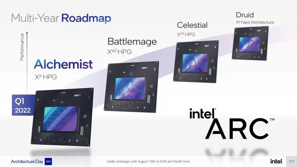
It’s Happening: Intel is hitting the gaming market with a big bang, finally bringing the fight to the same level as NVIDIA and AMD. The dedicated Intel ARC Alchemist GPU implements the Xe HPG graphics architecture and offers full support for DirectX 12 Ultimate, as well as other contemporary features such as XeSS (AI supersampling that rivals NVIDIA DLSS and AMD FSR) and much more, so let’s see what Intel has told us about it.
Intel Alchemist GPUs, under TSMC’s 6nm node
According to Intel, they have defined a new computer building block that serves as the foundation for the Xe architecture as part of this change. They have also taken the opportunity to update some of the names to stop talking about execution units; they were getting too big to be reasonable, and generational changes made comparisons difficult.
Thus, Intel has presented the XE cores, which include efficient arithmetic units, caches, and load storage logic. Arithmetic units include engines for traditional floating point operations, integer vectors along with acceleration, convolution, and matrix operations engines commonly found in AI workloads.
So Intel has decided to change the name of the execution unit to an even more technical nomenclature. Instead of EU, Intel now uses the following standard: the base unit of the Xe Alchemist GPUs will have 16 vector engines (256-bit) and 16 matrix engines (1024-bit), forming an Xe Core. Each of the Xe Cores will have its own Sampler, Geometry, Cachéw and a shared Pixel Backend; 4 Xe cores form a render segment, and each also has its own unit of ray tracing.
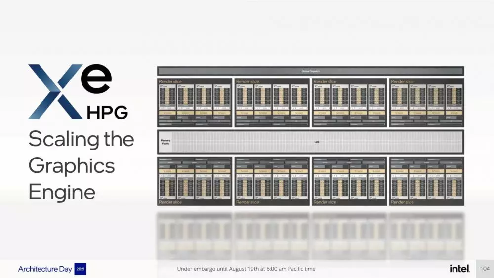
The first iteration of the Intel Xe HPG GPU will have 8 “parts” as you see in the slide above, each with 4 Xe cores. This constitutes a total vector / matrix count of 512 (8x4x16), and yes, that is exactly what we have known as EU until now. Assuming the base architecture is the same (it should be), we are still therefore talking about 4096 ALUs (512×8) on Intel Alchemist GPUs.
Additionally, TSMC has confirmed that Intel Xe HPG GPUs will be manufactured in its 6 nm lithography, which should give them a huge advantage in terms of energy efficiency and transistor density. This also means that it is quite likely that when they are launched on the market they will do so with a large volume of stock, since TSMC has no problem getting mass production out of this node.
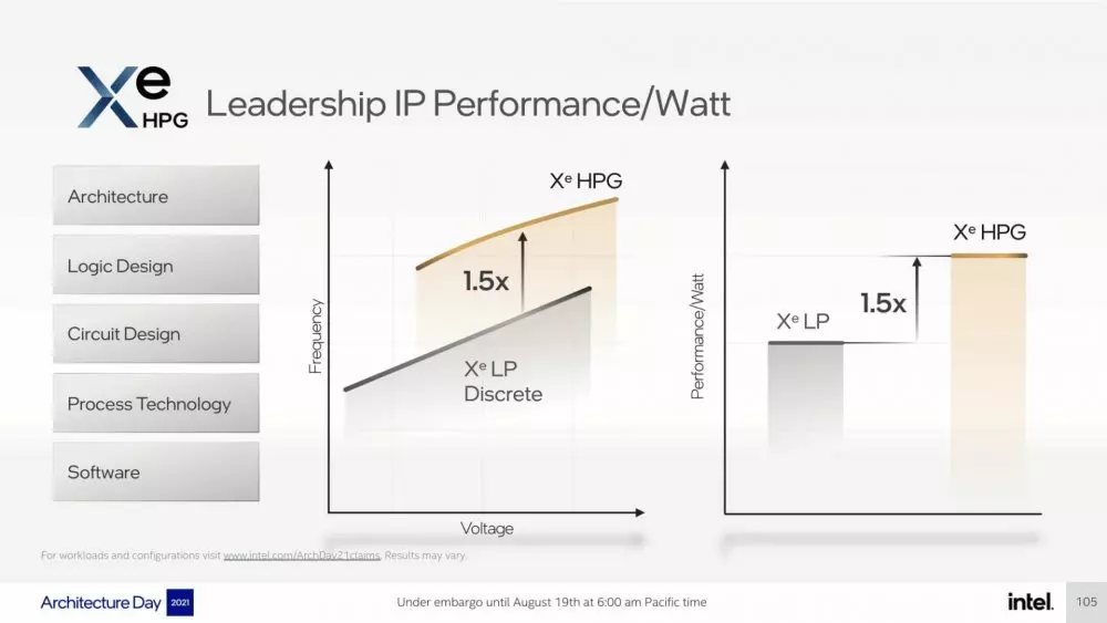
In principle, the Intel Xe HPG architecture that we will see released in the “Alchemist” Gaming GPUs will be able to reach clock speeds up to 1.5 times higher than what we saw with Xe LP, offering at the same time a performance per watt also 1, 5 times higher. This means that we will see operating speeds in the 2.1 GHz range considering that the dedicated Xe LP GPUs were running at 1.4 GHz, so we could be talking about a true rival for AMD and NVIDIA in the gaming graphics market. .
Intel Ponte Vecchio for servers, with 45 TFLOPS of power

In addition to talking about its upcoming and long-awaited GPUs Gaming Alchemist and more, Intel also spoke during its Architecture Day 2021 of server GPUs, an environment completely dominated by NVIDIA today but which, with the figures that Intel has presented, of course it endangers its hegemony.
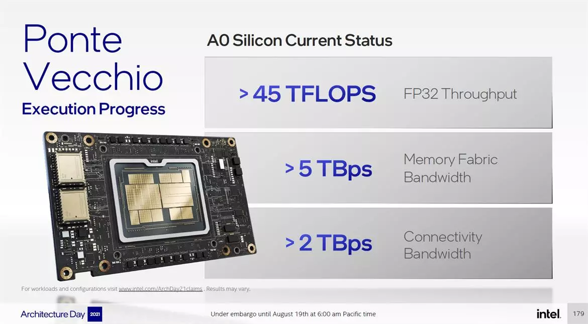
Ponte Vecchio has already managed to overcome the barrier of 45 TFLOPS single-precision computing performance on its current version of A0 silicon; This is a data center accelerator that is the first Xe-HPC-based processor to feature a multi-tile design, including Compute, Rambo, HBM and EMIB with a total of 47 tiles with 100 billion transistors.
Similar to the GPUs we’ve seen before, the Xe-HPC Xe Core is the building block of these GPUs, featuring 8 vector engines and 8 matrix engines. Compared to Xe-HPG, Ponte Vecchio will have fewer engines but will operate with much wider buses: 512 bits and 4096 bits respectively (for HPG, those figures are 256 and 1024 bits).
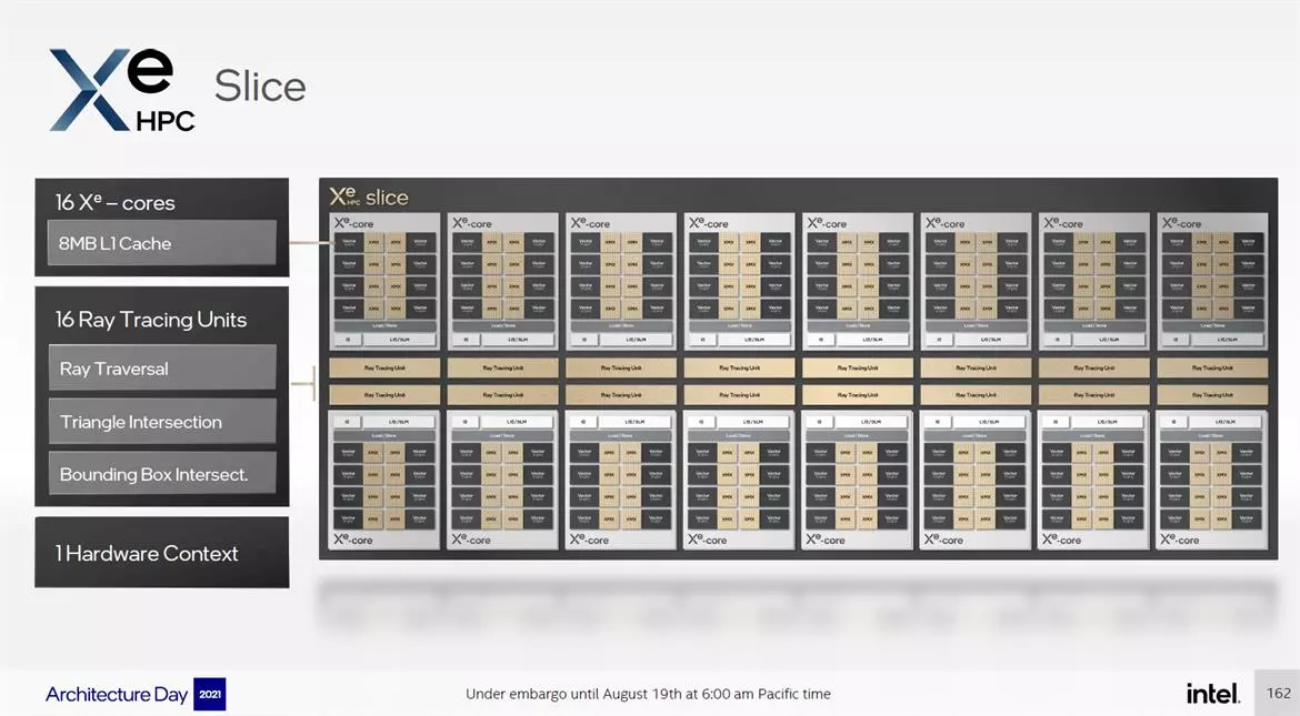
The Xe-HPC Slice is the main building block of these GPUs, combining 16 Xe Cores. What could be interesting is the fact that the Ponte Vecchio is equipped with ray tracing units, even though it is not a gaming-oriented GPU. Like HPG, each Xe Core is linked to a single Ray Tracing unit, and the purposes of these cores have been listed on the official slide as Cross Rays, Triangular Intersection, and Bounding Square Intersection. Being an accelerator for servers means, of course, that they are not designed for games.
Ponte Vecchio will be available in 1- and 2-stack configurations, which means specs up to 8 cores, 128 Xe Cores, and 128 ray tracing units. The 2-stack configuration will have no less than 8 HBM2e memory controllers.
The Intel Ponte Vecchio GPU has 5 different compute nodes, making it one of the most complex HPC accelerators on the market, if not the most. This may have some impact on server GPU provisioning, as in the event that any of these 5 vendors experience provisioning issues, so will these Intel GPUs.
Incidentally, Intel compares these GPUs to the NVIDIA A100 accelerator, and gets more than double the FP32 performance (45 TFLOPS vs 19.5 TFLOPS in NVIDIA’s solution). These GPUs are expected to make their formal debut from 2022, but the exact date is yet to be defined.