The market is changing and although we did not create it, computing as such is not the center of the world nor does it direct it, although it is an important part. There are thousands of industries that depend much more on other kinds of secondary and tertiary chips, which are in an even greater crisis than the one we are experiencing on PCs or consoles. Therefore, there is a new script twist that almost no one will like and that makes a lot of sense looking at the market, at least if we look from 2020 to 2025.
TrendForce: global logistics and manufacturing must be relocated
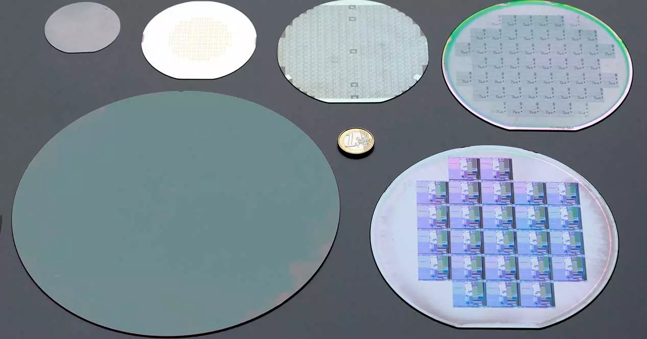
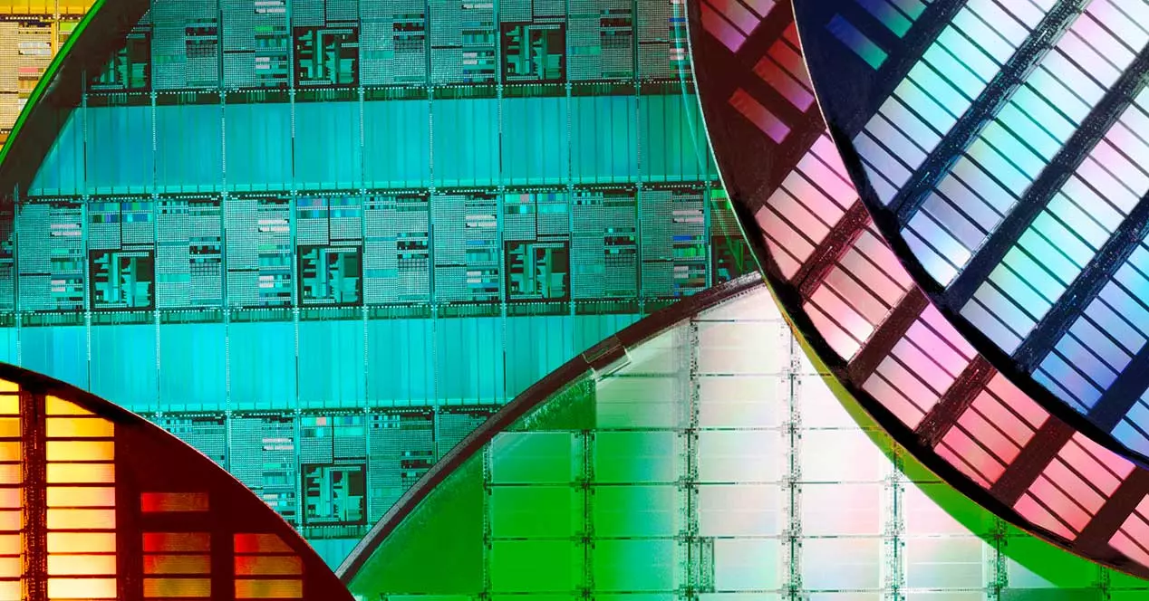
According to the study carried out by the firm, approximately 10% of the 10 largest foundries in the world is to work with 12-inch wafers. These wafers are called 300mm in diameter and logically they are the largest in the industry while waiting for the new versions (without specifying sizes yet). Therefore, high-volume, high-throughput players need them to maximize profits by launching more chips in the same size for each lithographic process that transistors are reduced.
All very well up to here and once we are introduced to this, we must know that the majority of the market does not work with 12 inches, but with 8 inches, especially because they are cheaper and the chips that are needed are small, achieving even greater profitability. But… The expansion capacity of the FAB for the 8 inches will only be one 3.3%, that is, in the period described above the capacity will increase by that percentage. Here we must include 5G chips, SoCs for smartphones and practically any piece of silicon used by the industry in general, from cars to control factories or smart LED bulbs.
Migration of chip wafers to 12 inches to increase production
 Intel, TSMC, Samsung and Global Foundations they are investing unimaginable amounts of money just a few years ago, where everything is focused on production capacity for 12-inch wafers given the size of the chips. But with the manufacturing shortage of 8″, manufacturers want to migrate from this size to its older brother and thereby alleviate the shortage of capacity, which is going to make what has been advanced with PC chips return to a previous point.
Such is the problem of wafer migration to satisfy the industry that reports indicate that this 2022 will not be the end of the semiconductor crisis for these reasons either. The dates already speak of the second semester of 2023 and even in 2024. That is, if there was little hope for 2022 and everything was set for 2023, we could now go 6 months further in time to early 2024, where some rumors would only say that these forecasts are optimistic.
Why such a delay if it’s just resizing? Because the densities are different in the wafers, which requires a redesign and conversion of the production process that will take months. The main problem is that we are talking about chips manufactured between 90nm and 55nm, easy for current scanners, but with larger sizes in total area due to its lower density. We will see how long it takes to go through, if not part, the entire production from the migration from 8 inches to 12 inches and how it affects the FABs.